Preparation method of semiconductor chip

A manufacturing method and semiconductor technology, applied in the fields of semiconductor/solid-state device manufacturing, electrical components, circuits, etc., can solve the problems of increased electron migration, high cost, and failure of electron migration test, so as to reduce the path and reduce the probability of occurrence. Effect

Inactive Publication Date: 2010-11-24
CSMC TECH FAB1
View PDF6 Cites 3 Cited by
  • Summary
  • Abstract
  • Description
  • Claims
  • Application Information

AI Technical Summary

Problems solved by technology

However, when trifluoromethane is used as an etching gas, more by-products are produced during the reaction, and heavier polymers will be formed on the side walls of the aluminum metal connection, and the fluorine ions contained in these polymers will corrode the aluminum metal. , causing the original grain boundary of the aluminum sidewall to be destroyed, and more grain boundaries are formed, so the path of electron migration will increase, and the probability of electron migration will increase accordingly, which will easily lead to the failure of electron migration test
[0007] In the prior art, when the electromigration test fails, it is mainly solved by adjusting the thickness of titanium or titanium nitride, but the effect is not obvious.
Or by using ion-implanted titanium to replace traditional physical vapor deposition titanium, but the cost is high

Method used


Image

  • Preparation method of semiconductor chip
  • Preparation method of semiconductor chip
  • Preparation method of semiconductor chip

Examples


Embodiment Construction

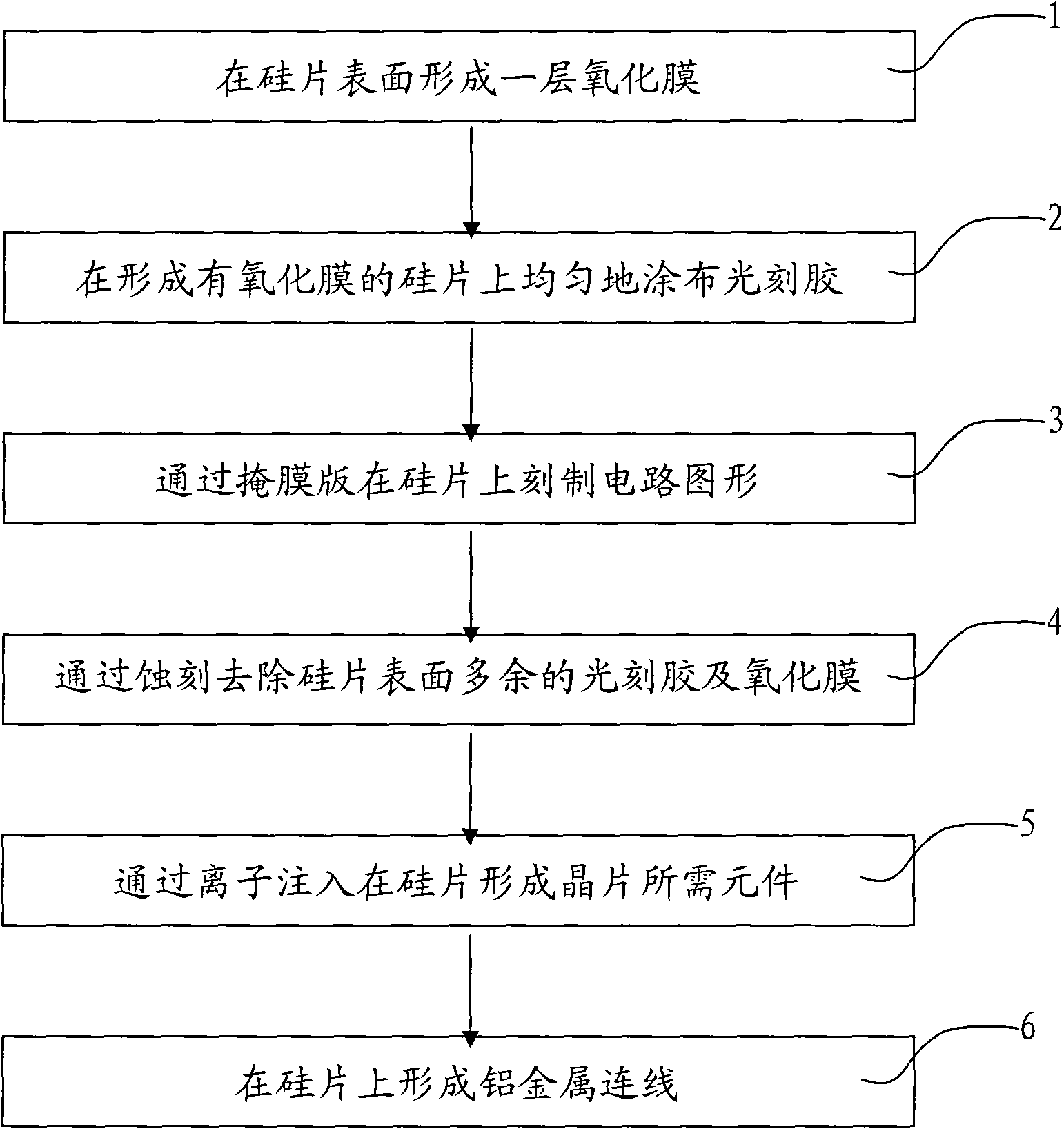
[0018] In view of the fact that the other steps of the semiconductor manufacturing method of the present invention are basically the same as the steps of the existing semiconductor chip manufacturing method, and these steps are not the invention point of the present invention, so other steps of the semiconductor manufacturing method (such as long Steps such as crystallization, cutting, etc.) are described in detail one by one, but only some main necessary steps in the semiconductor manufacturing method are listed.

[0019] see figure 1 As shown, it shows a flow chart of the semiconductor chip manufacturing method of the present invention. As shown in the figure, a semiconductor chip manufacturing method of the present invention includes the following steps:

[0020] Step 1: a step of first forming a uniform thin oxide film on the surface of the silicon wafer;

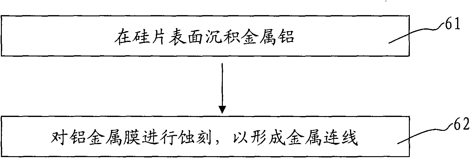
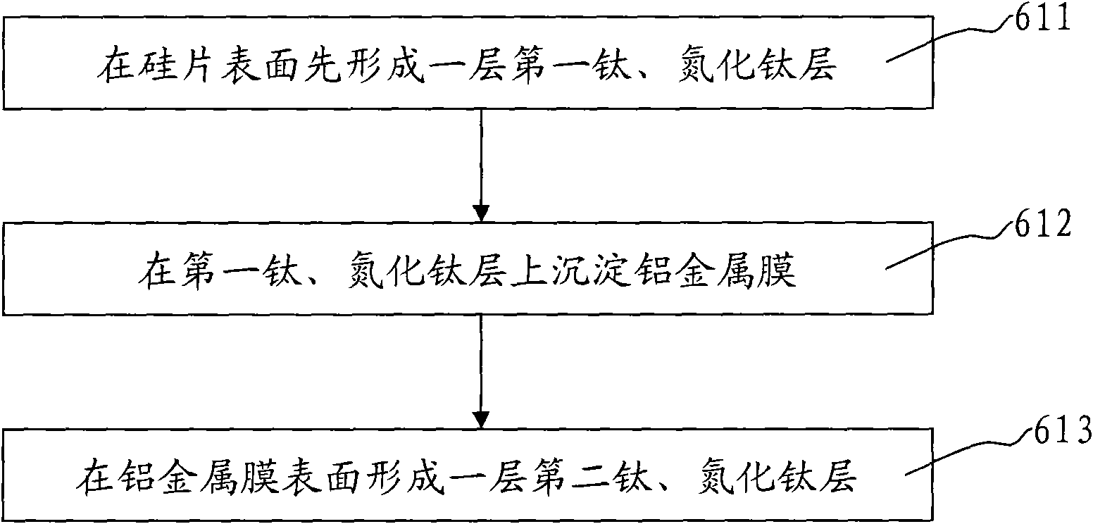
[0021] Step 2: then uniformly coating a photoresist on the silicon wafer formed with an oxide film to make the sili...


PUM


Abstract

The invention discloses a preparation method of a semiconductor chip. The method comprises the following steps: forming an oxide film on a silicon wafer, coating photoresist on the silicon wafer with the oxide film, using a mask to etch a circuit pattern on the silicon wafer with photoresist, etching to remove the residual photoresist and oxide film on the surface of the silicon wafer, forming elements required by the wafer through ion implantation, and forming metal wires on the silicon wafer, wherein the step of forming metal wires on the silicon wafer comprises the following steps: depositing metal aluminum on the surface of the wafer and etching metal aluminum to form the layout of wires. In the step of forming metal wires, when aluminum is etched, a mixed gas containing nitrogen is used as etching gas, the by-products of the reaction are less and a thermally stable film is formed, thus protecting the aluminum side wall, reducing the path of electron transfer and lowering the probability of electron transfer.

Description

【Technical field】 [0001] The invention relates to a semiconductor manufacturing method, in particular to a method for improving the semiconductor metal connection etching method so as to change the electromigration performance of the semiconductor chip metal connection. 【Background technique】 [0002] Electron migration (EM) is an effect in which metal atoms are displaced due to the impact of a stream of electrons. When a large current passes through the metal wire, the electrostatic force drives the electrons to move from the cathode to the anode, and the high-speed electrons exchange energy with the metal atoms. The atoms are subjected to violent electron impact (the so-called electronic wind force), but the metal atoms simultaneously It also receives the electrostatic field force in the opposite direction. When the current density in the metal wire is high, a large number of electrons moving to the anode collide with the atoms, so that the electron wind force received by ...

Claims


Application Information

Patent Timeline
IPC IPC(8): H01L21/768C23F1/12
Inventor 许宗能任小兵薛浩
Owner CSMC TECH FAB1
Why Eureka
Try Eureka