Fabricating method of InGaN (Indium-Gallium-Nitrogen) semiconductor photoelectrode
A manufacturing method and photoelectrode technology, applied in the direction of electrodes, electrolysis process, electrolysis components, etc., can solve the problems of small contact area of electrolyte and low reaction efficiency, and achieve the effect of increasing effective contact area, improving conversion efficiency and reducing reflection.
- Summary
- Abstract
- Description
- Claims
- Application Information
AI Technical Summary
Problems solved by technology
Method used
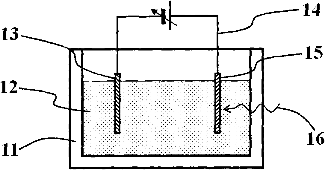
Image

Examples
Embodiment 1
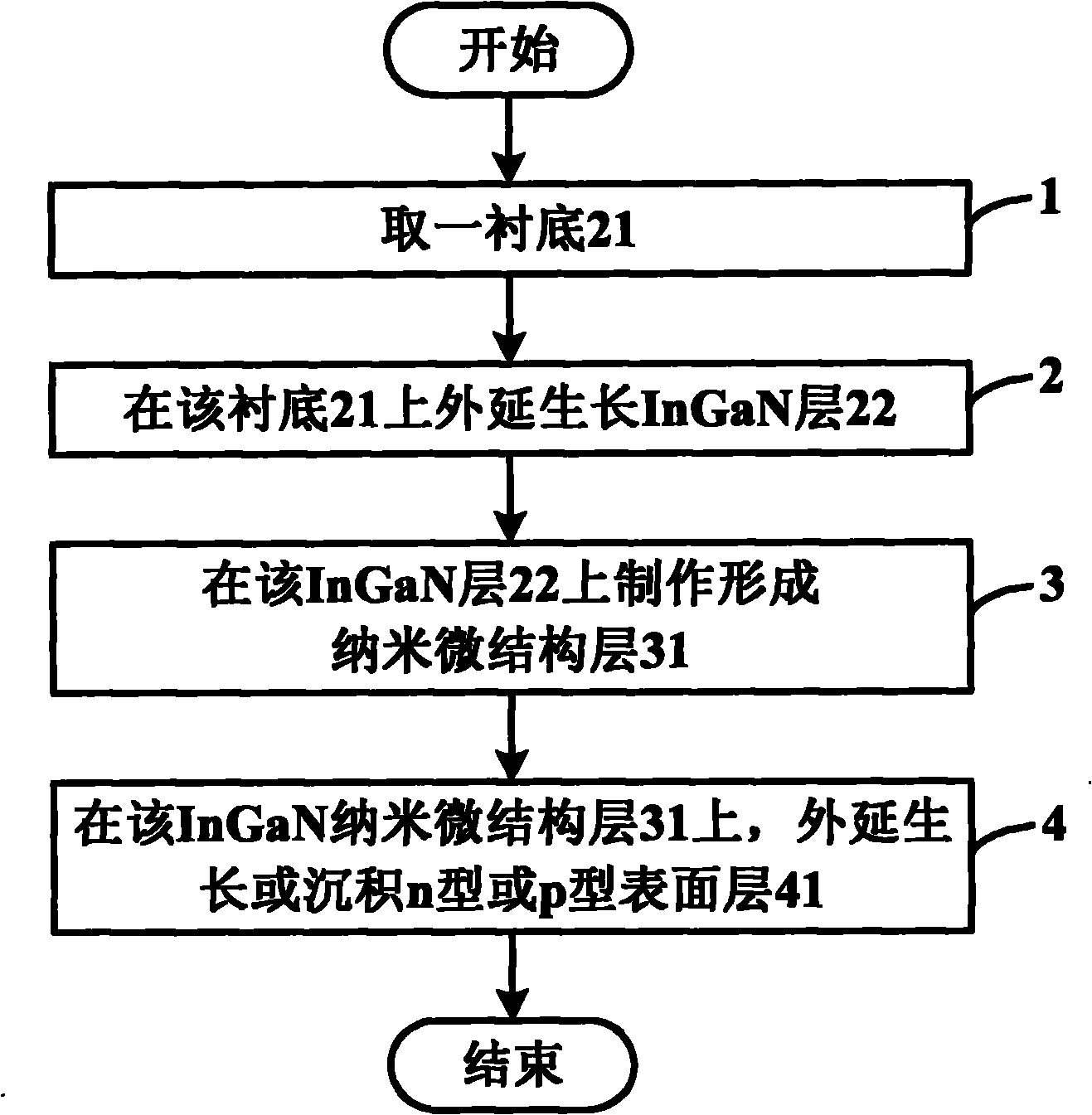
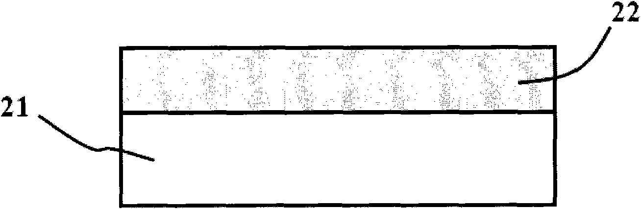
[0046] Embodiment one: see Figure 3 ~ Figure 5 shown. The InGaN layer 22 is epitaxially grown on the substrate 21 by metal organic chemical vapor deposition (MOCVD), wherein the substrate 21 is a sapphire substrate; the InGaN layer 22 is an n-type GaN epitaxial layer with a thickness of 3000nm; Deposit 200nm thick SiO on layer 22 2 Dielectric film; then vapor-deposit metal Ni with a thickness of 15nm on the dielectric film, and gather metal Ni into metal islands with a diameter of about 200 nanometers by means of rapid annealing. Using the metal island as a mask material, etch the InGaN layer 22 with an etching depth of 100nm, thereby producing a nano-microstructure 31, wherein the nano-microstructure is a GaN nano-column; A surface layer 41 is grown on the epitaxial wafer surface of the structure 31, and the surface layer 41 is n-type In with a thickness of 200 nm. 0.1 Ga 0.9 N layer to finally obtain an InGaN semiconductor photoelectrode.
Embodiment 2
[0047] Embodiment two: see Figure 3 ~ Figure 5 shown. The InGaN layer 22 is epitaxially grown on the substrate 21 by metal organic chemical vapor deposition (MOCVD), wherein the substrate 21 is a sapphire substrate; the InGaN layer 22 is an n-type GaN epitaxial layer with a thickness of 3000nm; Deposit 200 nm thick SiO on layer 22 2 Dielectric film; then vapor-deposit metal Ni with a thickness of 15nm on the dielectric film, and gather metal Ni into metal islands with a diameter of about 200nm by means of rapid annealing. Using the metal island as a mask material, etch the InGaN layer 22 with an etching depth of 100nm, thereby producing a nano-microstructure 31, wherein the nano-microstructure is a GaN nano-column; A surface layer 41 is grown on the epitaxial wafer surface of the structure 31, and the surface layer 41 is p-type In with a thickness of 200 nm. 0.1 Ga 0.9 N layer to finally obtain an InGaN semiconductor photoelectrode.
Embodiment 3
[0048] Embodiment three: see Figure 3 ~ Figure 5 shown. Deposit 200 nm thick SiO on the substrate 21 2 A dielectric film, wherein the substrate 21 is an n-type GaN substrate material; then metal Ni is evaporated on the dielectric film with a thickness of 15nm, and the metal Ni is aggregated into metal islands with a diameter of about 200nm by rapid annealing. Using the metal island as a mask material, etch the substrate 21 with an etching depth of 100nm, thereby producing a nano-microstructure 31, wherein the nano-microstructure 31 is a GaN nanocolumn; A surface layer 41 is grown on the epitaxial wafer surface of the microstructure 31, and the surface layer 41 is n-type In with a thickness of 200 nm. 0.1 Ga 0.9 N layer to finally obtain an InGaN semiconductor photoelectrode.
PUM
| Property | Measurement | Unit |
|---|---|---|
| thickness | aaaaa | aaaaa |
| thickness | aaaaa | aaaaa |
| thickness | aaaaa | aaaaa |
Abstract
Description
Claims
Application Information
 - R&D
- Intellectual Property
- Life Sciences
- Materials
- Tech Scout
- Unparalleled Data Quality
- Higher Quality Content
- 60% Fewer Hallucinations
Browse by: Latest US Patents, China's latest patents, Technical Efficacy Thesaurus, Application Domain, Technology Topic, Popular Technical Reports.
© 2025 PatSnap. All rights reserved.Legal|Privacy policy|Modern Slavery Act Transparency Statement|Sitemap|About US| Contact US: help@patsnap.com