Nano-imprint template and preparation method thereof

A nano-imprinting and template technology, applied in optical mechanical equipment, photo-engraving process of pattern surface, optics, etc., can solve the problems of poor crush resistance, high cost, brittle nano-imprint template, etc., to achieve crush resistance The effect of good performance, simple method and low cost

Active Publication Date: 2010-12-22
TSINGHUA UNIV +1
View PDF0 Cites 19 Cited by
  • Summary
  • Abstract
  • Description
  • Claims
  • Application Information

AI Technical Summary

Problems solved by technology

[0006] However, the existing nanoimprint templates are usually made of inert materials with high hardness, high thermal conductivity, low expansion coefficient, and strong corrosion resistance, such as silicon, silicon dioxide, silicon carbide, or silicon nitride.
Nanoimprint templates using the above materials are usually made by electron beam etching. However, the preparation of nanoimprint templates using the above-mentioned high-hardness materials is complicated and requires strict conditions, resulting in high costs.
Moreover, the nanoimprint templates prepared by the above materials are brittle, have poor crush resistance, and are relatively easy to be damaged.

Method used


Image

  • Nano-imprint template and preparation method thereof
  • Nano-imprint template and preparation method thereof
  • Nano-imprint template and preparation method thereof

Examples


no. 1 example

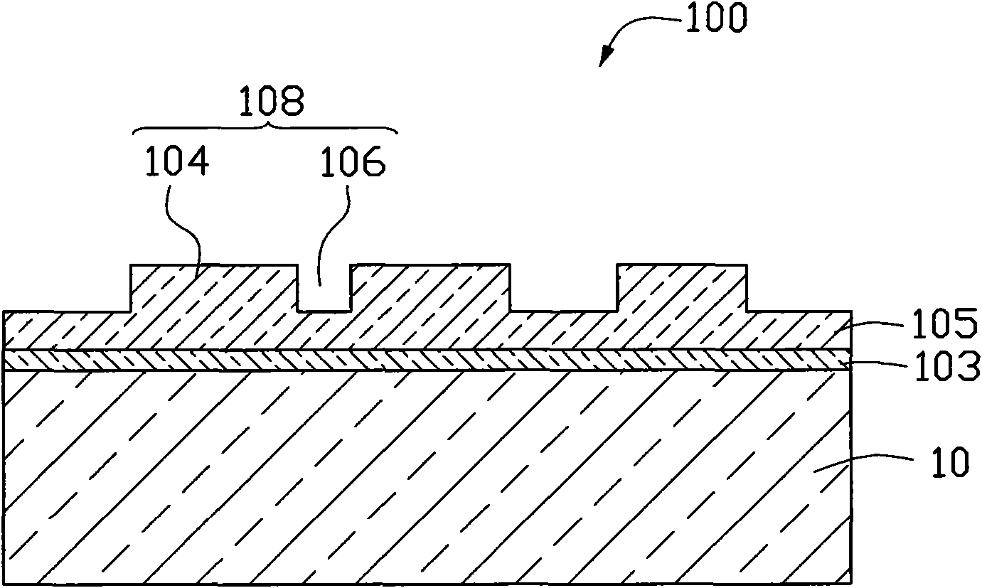
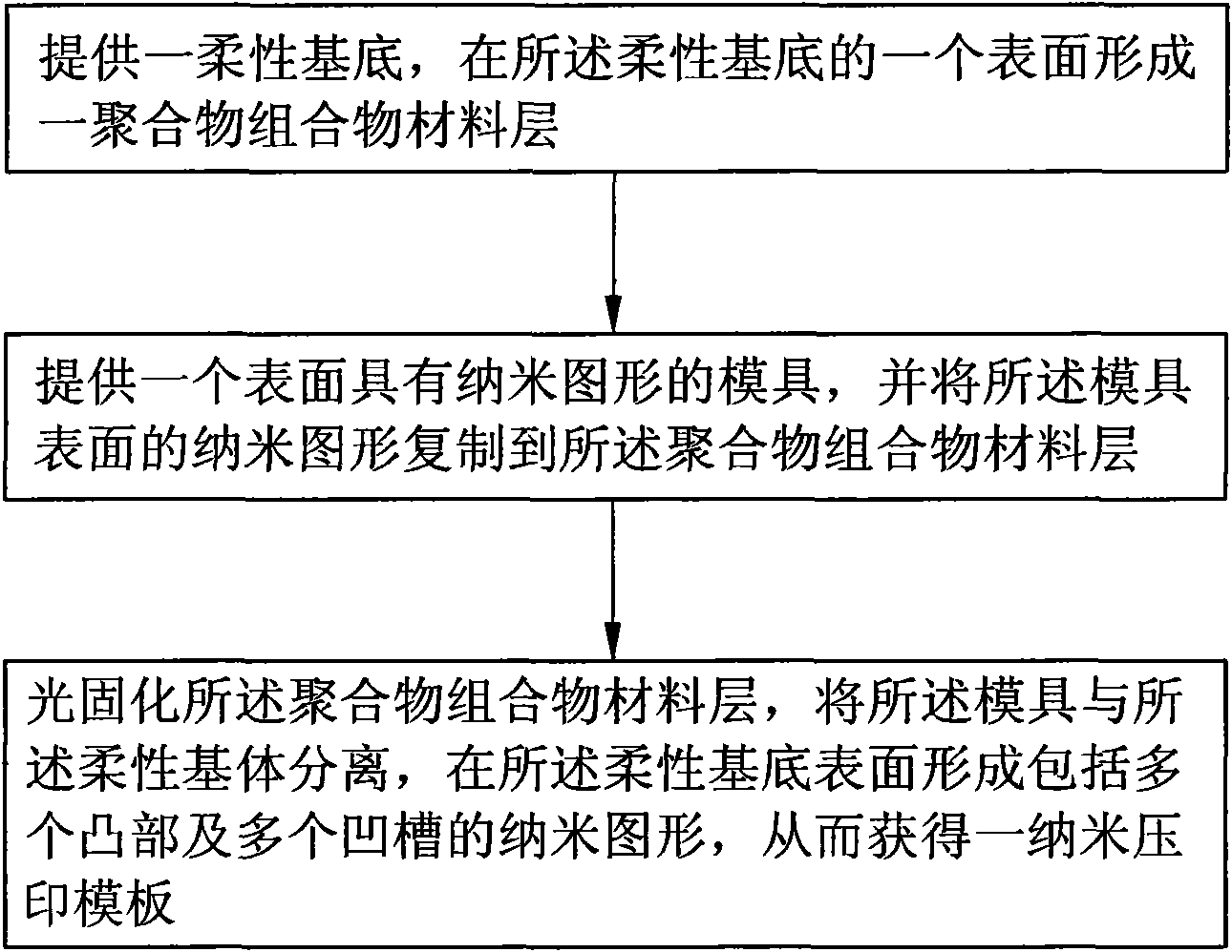
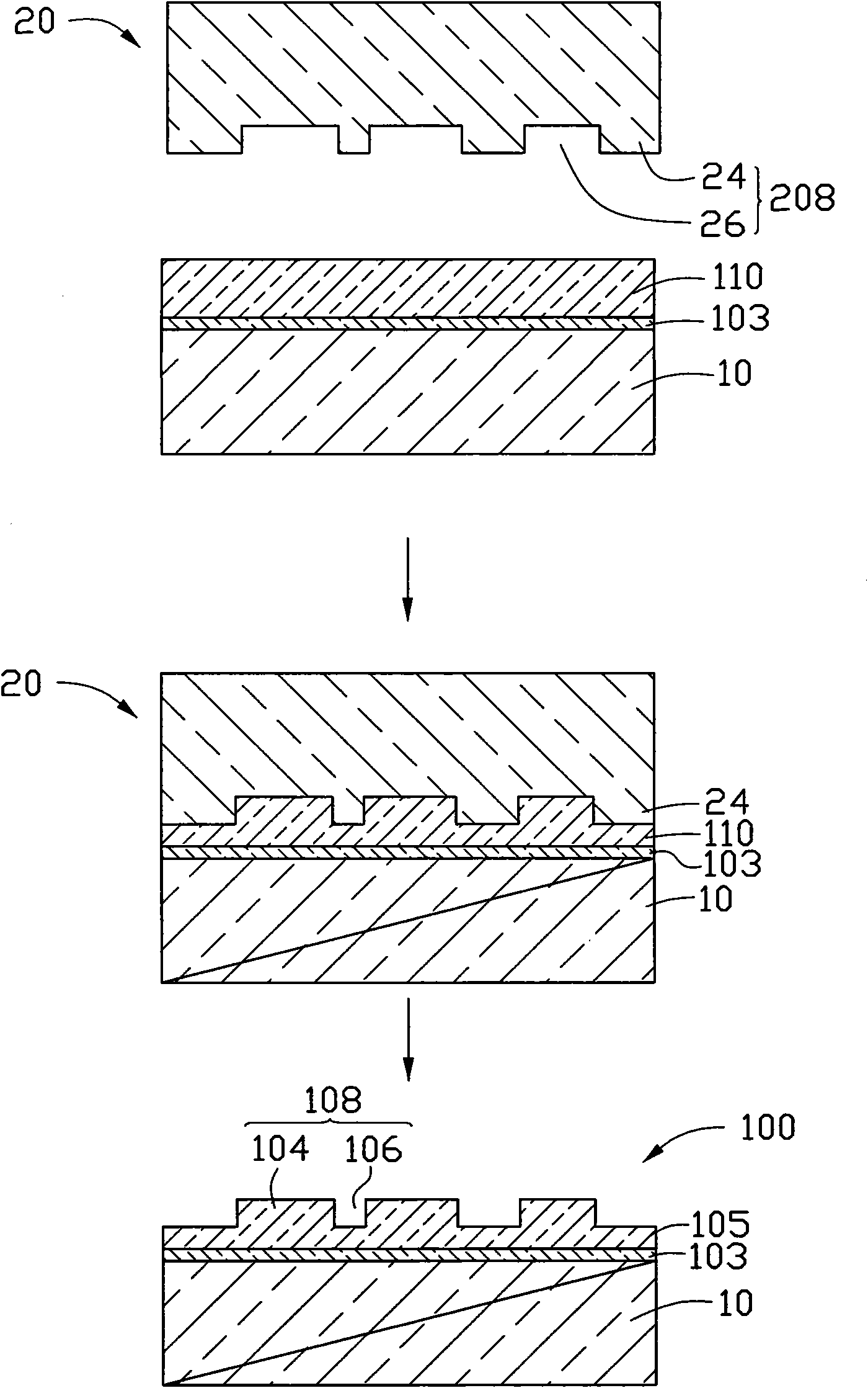
[0028] The present invention further provides a method for preparing the nanoimprint template. see figure 2 and image 3 , the first embodiment of the preparation method of the nanoimprint template includes the following steps:

[0029] In step 1, a flexible substrate 10 is provided, and a polymer composition material layer 110 is formed on one surface of the flexible substrate 10 .

[0030]The flexible base 10 is a flat plate, and its shape and size are not limited, and it can be a circular flat plate, a square flat plate, etc. The material of the flexible substrate 10 is a flexible transparent polymer material, specifically, it can be selected from silicone rubber, polyurethane, epoxy resin, polymethyl methacrylate, polyethylene terephthalate (PET) A blend of one and any of its components. In this embodiment, the flexible base 10 is a circular flat plate with the size of a 4-inch silicon wafer, and the material of the flexible base 10 is polyethylene terephthalate (PET)...


PUM

PropertyMeasurementUnit
sizeaaaaaaaaaa
thicknessaaaaaaaaaa

Abstract

The invention provides a nano-imprint template which comprises a flexible substrate and a polymer layer formed on a surface of the flexible substrate, wherein, a nano-graph is formed on a surface of the polymer layer away from the flexible substrate; and the polymer layer is a solidified cross-linked substance composed of a hyperbranched lower polymer, perfluoro polyether, methyl methacrylate and an organic diluent. The invention further provides a preparation method of the nano-imprint template.

Description

technical field [0001] The invention relates to a nano-imprint template and a preparation method thereof, in particular to an ultraviolet nano-imprint template and a preparation method thereof. Background technique [0002] In the prior art, when making various semiconductor devices, it is often necessary to make nano-patterns with microstructures ranging from tens of nanometers to hundreds of nanometers. The fabrication method of the nano-pattern with the above-mentioned fine structure mainly includes the lithography method of light or electron beam: at first, use the radiation line or the electron beam that pass through the mask or scanning focus to irradiate the photoresist composition or the mask, the above-mentioned radiation The line or electron beam will change the chemical structure of the resist in the exposed area; then, the resist in the exposed area or outside the exposed area is removed by etching to obtain a specific pattern. [0003] In order to adapt to the ...

Claims


Application Information

Patent Timeline
Patent Type & Authority Applications(China)
IPC IPC(8): G03F1/00G03F7/00
Inventor 朱振东李群庆张立辉陈墨
Owner TSINGHUA UNIV
Why Eureka
Try Eureka