Semiconductor element module and method for manufacturing the same

A manufacturing method and semiconductor technology, applied in the fields of semiconductor/solid-state device manufacturing, semiconductor devices, semiconductor/solid-state device components, etc., can solve the problems of reduced thermal conductivity, inability to ensure reliability, and inability to obtain heat dissipation performance

Inactive Publication Date: 2011-01-12
MITSUBISHI HEAVY IND LTD
View PDF1 Cites 6 Cited by
  • Summary
  • Abstract
  • Description
  • Claims
  • Application Information

AI Technical Summary

Problems solved by technology

Therefore, there is a problem that the expected heat dissipation performance cannot be obtained
[0009] In addition, in the above-mentioned module structure, the limitations of heat resistance, thermal cycle resistance, and vibration resistance of solder and lead wires used for wiring, resin used for packaging, etc. determine the limits of improvement of the entire module
Since the heat resistance, heat cycle resistance, and vibration resistance required for electric vehicles, etc. cannot be satisfied, these module structures cannot ensure sufficient reliability
For example, the components inside the module may be intact, but the wiring may be damaged, thereby impairing the function of the module as a whole, thus reducing the reliability and life of the module
[0010] In addition, with the above-mentioned module structure, etc., there are problems in achieving both heat dissipation performance and reliability at the point of bonding between the substrate and the element and / or between the substrate and the heat sink
For example, the use of adhesives for bonding can lead to issues with slightly lower thermal conductivity and increased process steps
Bonding using diffusion bonding or anodic bonding may have the following problems: the types of materials used for bonding objects are limited, and since heating is involved in bonding, a certain cooling time is required, and it also causes thermal influence on the module (generates thermal stress)

Method used


Image

  • Semiconductor element module and method for manufacturing the same
  • Semiconductor element module and method for manufacturing the same
  • Semiconductor element module and method for manufacturing the same

Examples


Embodiment 1

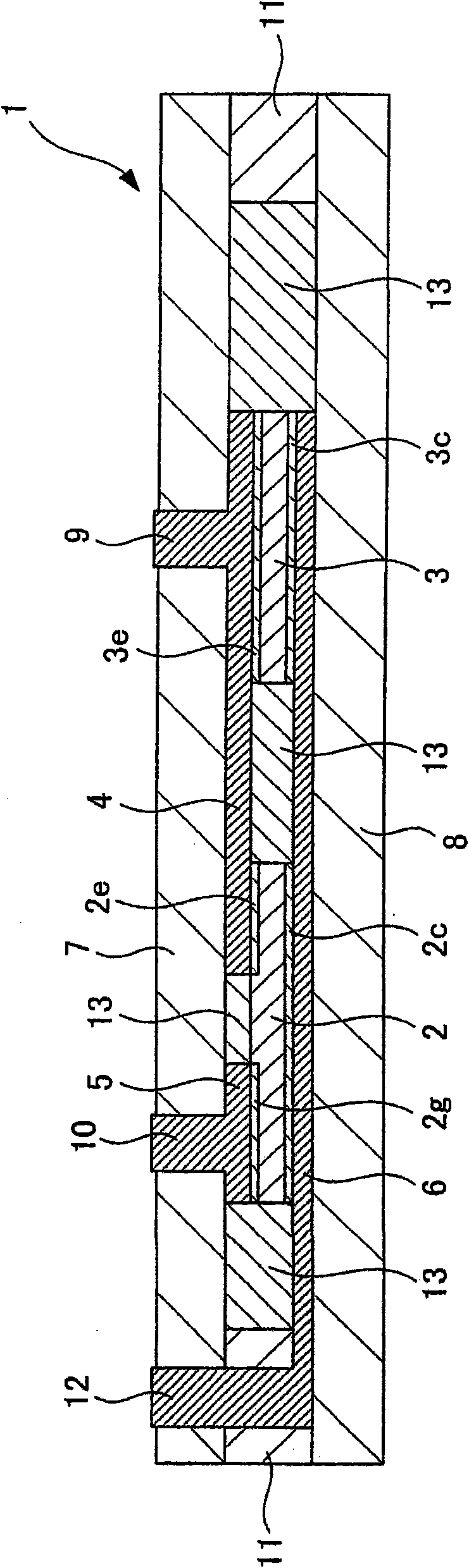
[0050] figure 1is a configuration diagram showing an exemplary embodiment of the semiconductor element module of the present invention. Note that the semiconductor element module 1 of the present embodiment is configured to include therein the insulated gate bipolar transistor 2 and the diode 3 as semiconductor elements, but may also be configured to include therein at least one semiconductor element. The semiconductor element module 1 is particularly suitable for semiconductor elements that generate a large amount of heat.

[0051] Such as figure 1 As shown, the semiconductor element module 1 of the present embodiment includes an insulated gate bipolar transistor 2, a diode 3, a flat ceramic substrate 7 (second insulating substrate), a flat ceramic substrate 8 (first insulating substrate) and Sealing member 11. The insulated gate bipolar transistor 2 and the diode 3 each have flat electrode surfaces formed on both surfaces thereof. The ceramic substrate 7 has high thermal...

Embodiment 2

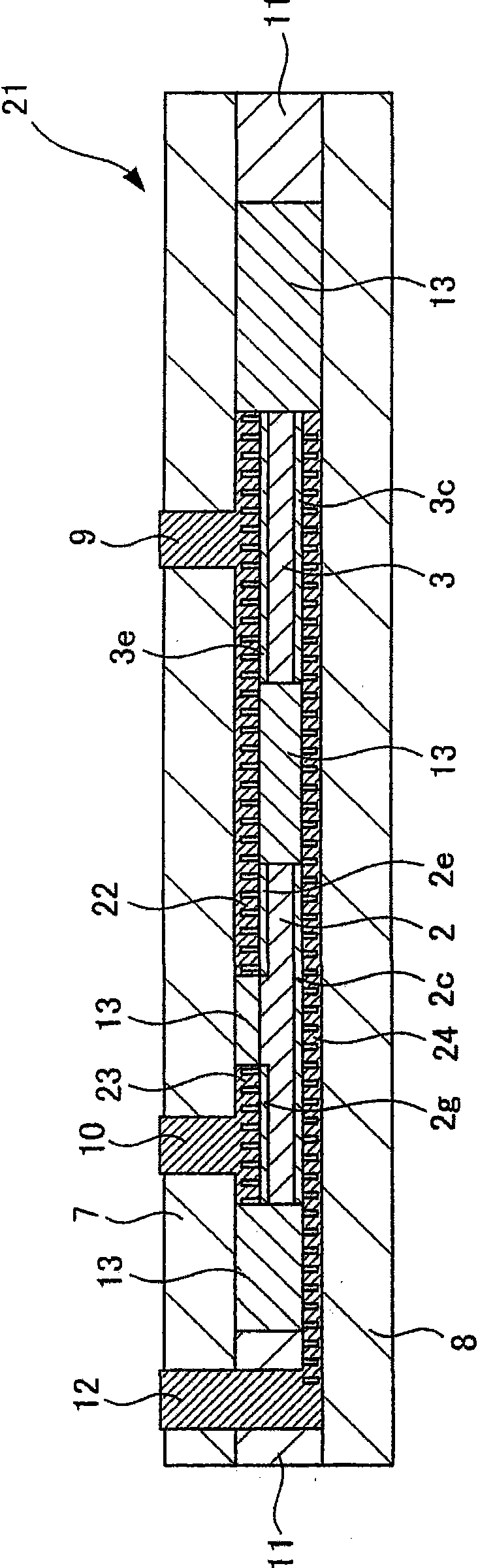
[0072] FIG. 2 is a structural diagram showing another exemplary embodiment of the semiconductor element module of the present invention. Note that the same reference numerals are used to denote the same as in Embodiment 1 ( figure 1 ) that are the same as the respective components of the semiconductor element module shown in ), and their repeated descriptions are omitted.

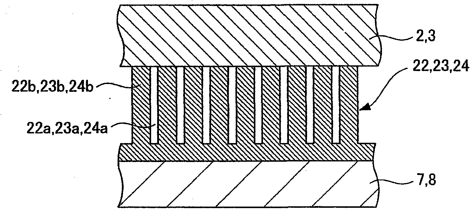
[0073] As shown in FIG. 2( a), the semiconductor element module 21 of this embodiment has substantially the same structure as that of Embodiment 1, except that the collector electrode surface 2c, the emitter electrode surface 2c, and the emitter electrode are arranged on the surface of the insulated gate bipolar transistor 2. Surface 2e and gate electrode surface 2g and electrode surface 3c and electrode surface 3e provided on the surface of diode 3 respectively form wiring circuit layers 22, 23, 24 of ceramic substrates 7, 8.

[0074] As with the wiring circuit layers 4 and 5 in Embodiment 1, on the inner...

Embodiment 3

[0084] Figure 4 is a structural diagram showing another exemplary embodiment of the semiconductor element module of the present invention. Note that the same reference numerals are used to denote the same as Embodiments 1 and 2 ( figure 1 Components that are the same as those of the semiconductor element module shown in 2), and their repeated descriptions are omitted.

[0085] The semiconductor element module of this embodiment is obtained by directly bonding a heat sink 41 (cooling means) made of metal excellent in heat dissipation to Embodiment 1 or 2 ( figure 1 Or 2) The ceramic substrate 8 of the semiconductor element module 1 or 21 shown.

[0086] Specifically, the bonding surface of the ceramic substrate 8 of the semiconductor element module 1 or 21 and the bonding surface of the heat sink 41 are activated by physical sputtering through ion beam irradiation or the like, and then pressure-welded to each other at room temperature, thereby The bonding surfaces are bonde...


PUM

PropertyMeasurementUnit
thicknessaaaaaaaaaa

Abstract

Provided are a semiconductor element module which is excellent in terms of thermal connection and electric connection, the cooling performance of which can be fully secured, and which is highly reliable, and a method for manufacturing the same. The semiconductor element module comprises an IGBT (2) and a diode (3) on both surfaces of which an electrode is formed, a ceramic substrate (7) on the surface of which wiring circuit layers (4, 5) which are bonded to one surface of the IGBT (2) and the diode (3) are formed and the thermal conductivity of which is high, a ceramic substrate (8) on the surface of which a wiring circuit layer (6) which is bonded to the other surfaces of the IGBT (2) and the diode (3) is formed and the thermal conductivity of which is high, and a sealing member (11) which is sandwiched between the outer edges of the ceramic substrates (7, 8) and with which the inside is sealed. These members are bonded by an ordinary temperature bonding method.

Description

technical field [0001] The present invention relates to a semiconductor element module and a manufacturing method thereof, and is suitable for semiconductor elements having high output such as power transistors. Background technique [0002] For example, power semiconductor elements with large output and high heat generation, such as insulated gate bipolar transistors (insulated gate bipolar transistors, IGBTs), need to be cooled to ensure their functional reliability and lifetime. In recent years, the use of such power semiconductor elements has been expanding, for example, they have been used to control motors of electric vehicles and the like. Therefore, in addition to improving output, improvements in reliability, life, and the like are required. [0003] Patent Document 1: Japanese Patent Application Publication No. Heisei 6-188363 [0004] Patent Document 2: International Patent Application Publication No. 98 / 43301 [0005] The problem to be solved by the present in...

Claims


Application Information

Patent Timeline
Patent Type & Authority Applications(China)
IPC IPC(8): H01L23/12H01L21/52H01L25/07H01L25/18
CPCH01L2924/0002H01L24/19H01L23/3735H01L23/051H01L25/18H01L23/5385H01L2924/13055H01L25/072H01L2924/01079H01L2924/12042H01L2924/1305H01L2924/15787H01L2924/351H01L2924/00
Inventor 上野大司和田太郎舩山正宏黑田能克近藤雄一小林真一中野浩儿藤原谦二竹下照雄
Owner MITSUBISHI HEAVY IND LTD
Why Eureka
Try Eureka