Method for preparing quasi three-dimensional photonic crystals on potassium titanyl oxygenic phosphate crystals

A technology of potassium titanyl phosphate and photonic crystal, which is applied in the direction of light guide, optics, optical components, etc.

Inactive Publication Date: 2011-01-19
SHANDONG UNIV
View PDF1 Cites 10 Cited by
  • Summary
  • Abstract
  • Description
  • Claims
  • Application Information

AI Technical Summary

Problems solved by technology

The American academic journal AppliedPhysicsLetters has announced the method (MatthieuRoussey, Appl. Phys. Lett. 87, 241101 (2005)) combining the annealing proton exchange technology and the FIB system to make photonic crystals on lithium niobate crystals, but the ion beam technology is currently Combining with FIB technology to fabricate photonic crystals on KTP crystals that can confine beam transmission in three dimensions, there is no information related to

Method used


Image

  • Method for preparing quasi three-dimensional photonic crystals on potassium titanyl oxygenic phosphate crystals
  • Method for preparing quasi three-dimensional photonic crystals on potassium titanyl oxygenic phosphate crystals
  • Method for preparing quasi three-dimensional photonic crystals on potassium titanyl oxygenic phosphate crystals

Examples


Embodiment 1

[0021] A method for preparing a quasi-three-dimensional photonic crystal structure on a potassium titanyl phosphate crystal, the method is:

[0022] 1) Prepare and process the sample: the sample is a Z-cut KTP crystal with a size of 10mm×10mm and a thickness of 2mm; the surface of the sample and the two opposite end faces are optically polished, and then cleaned with deionized water, alcohol and acetone;

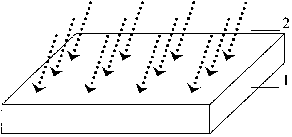
[0023] 2) Ion implantation to form a planar waveguide structure: put the cleaned KTP sample into the accelerator target chamber for light ion or heavy ion implantation, the implantation conditions are: light ion H + , energy: 400keV; heavy ion C + , energy: 1MeV; dose is light ion 5×10 16 Ions / cm², heavy ions 1×10 13 Ions / cm2; beam current is 20nA;

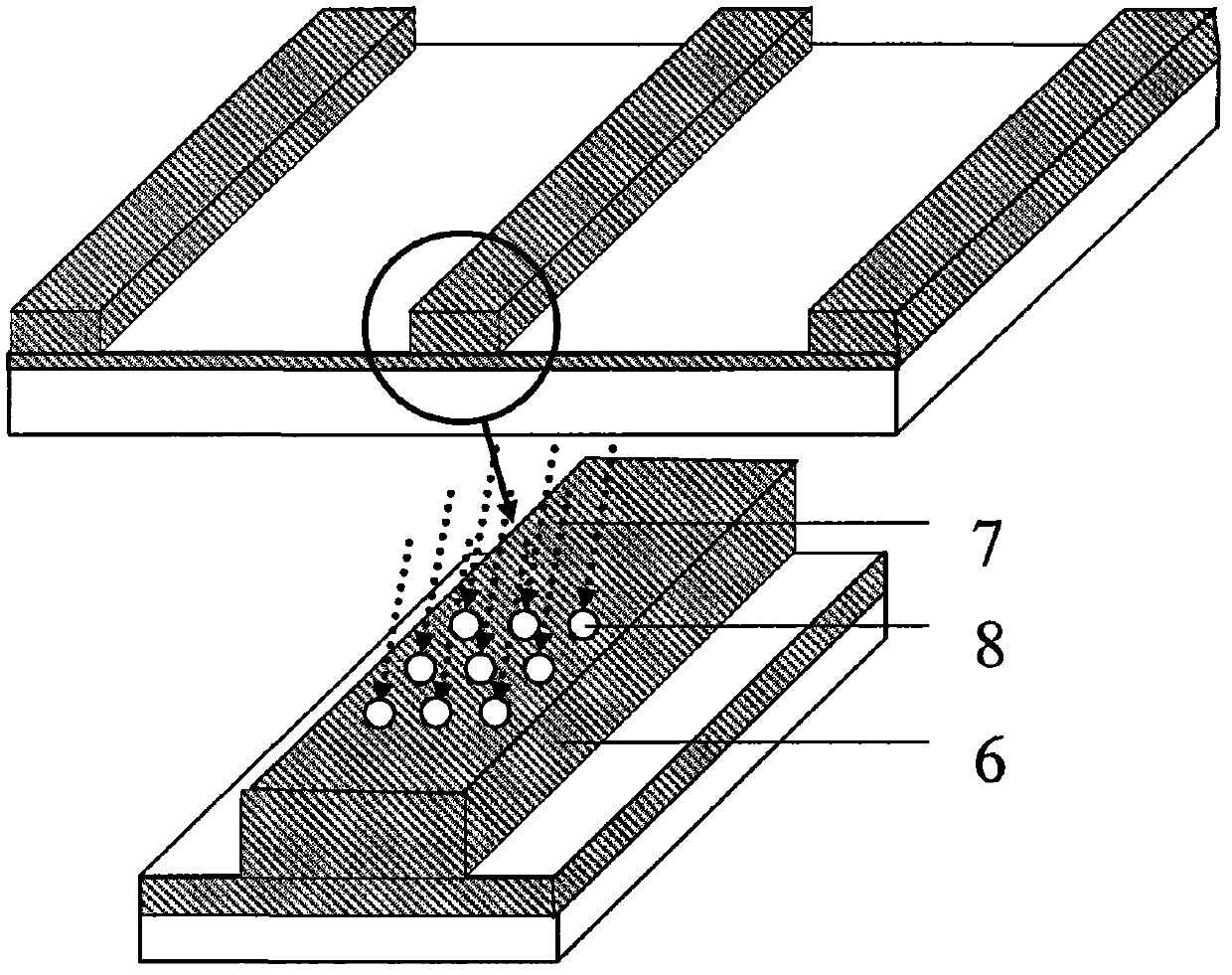
[0024] 3) Prepare a photoresist mask on the planar waveguide structure: Spin and coat BP218 photoresist on the planar waveguide structure with a homogenizer. Expose a 5 micron mask, then develop it with a positive photoresis...

Embodiment 2

[0029] A method for preparing a quasi-three-dimensional photonic crystal structure on a potassium titanyl phosphate crystal, the method is the same as in Example 1, the difference is that in step 2), the implantation condition is: light ion He + , energy: 500keV; heavy ion O + , energy: 1.5MeV; in step 3), the mask plate exposure with a shading stripe spacing of 30 microns and a shading stripe width of 10 microns; in step 4), the Ar ion beam energy is 1.5KeV, and the beam current density is 30 milliamperes / cm, etch to form a KTP ridge waveguide with a width of 10 microns and a depth of 0.8 microns; in step 6), the hole pitch of the quasi-three-dimensional photonic crystal is 600 nm, and the hole radius is 200 nm.


PUM

PropertyMeasurementUnit
energyaaaaaaaaaa
depthaaaaaaaaaa
thicknessaaaaaaaaaa

Abstract

The invention discloses a method for preparing quasi three-dimensional photonic crystals on potassium titanyl oxygenic phosphate (KTP) crystals, which belongs to the technical field of optoelectronic device manufacturing. The preparation method comprises: firstly, cutting the KTP crystals to make a 10mm*10mm*2mm sample, and polishing the surfaces and two opposite end faces of the sample optically; placing the sample in an accelerator target room and performing ion implantation to form a planar optical waveguide; washing the sample with deionized water, ethanol and acetone, rotationally coating BP218 photoresist on the sample, exposing, developing and hardening film to form a photoresist strip mask; making a ridge waveguide by etching with an Ar ion beam; and plating a conductive film on the surface of the ridge waveguide, etching a submicron photonic crystal structure in a ridge waveguide area by using an FIB system, and obtaining the submicron quasi three-dimensional photonic crystals with high performance by regulating system parameter and working conditions. The method can realize the three-dimensional restraining of light beams and can be used for manufacturing photonic crystal filters, beam splitters, reflectors and other photoelectric devices.

Description

technical field [0001] The invention relates to a method for preparing a quasi-three-dimensional photonic crystal structure on a potassium titanyl phosphate crystal, and belongs to the technical field of optoelectronic device preparation. Background technique [0002] Potassium titanyl phosphate (KTiOPO 4 , referred to as KTP) crystal is a nonlinear optical crystal with excellent performance. It has the advantages of large nonlinear coefficient, high electro-optical coefficient, high frequency doubling efficiency, and stable chemical properties. It is an important material for making optoelectronic devices. More applications. [0003] Focused ion beam system (FIB) integrates the processes of morphology observation, positioning sample preparation, thin film deposition and maskless etching. It has excellent maskless and high-resolution etching capabilities, and has become important technical means. [0004] Photonic crystals have many specific physical phenomena, providing ...

Claims


Application Information

Patent Timeline
Patent Type & Authority Applications(China)
IPC IPC(8): G02B6/122G02B6/134G02B6/136
Inventor 刘鹏赵金花黄庆管婧王雪林
Owner SHANDONG UNIV
Why Eureka
Try Eureka