Method for manufacturing double diffusion type optical avalanche diode with incident light on back surface by adopting epitaxial equipment

A double diffusion, avalanche tube technology, applied in electrical components, circuits, semiconductor devices, etc., can solve the problems of PN junction interface depression, inability to achieve doping, slow diffusion rate, etc., to reduce series resistance, suppress surface electric field, avoid absorption effect

Active Publication Date: 2011-01-19
WUHAN HUAGONG GENUINE OPTICS TECH
View PDF5 Cites 21 Cited by
  • Summary
  • Abstract
  • Description
  • Claims
  • Application Information

AI Technical Summary

Problems solved by technology

The front light input type needs to use InGaAs as the ohmic contact layer. During the diffusion process, the diffusion rate of InGaAs is slower than that of indium phosphide, which makes the PN junction interface concave

Method used


Image

  • Method for manufacturing double diffusion type optical avalanche diode with incident light on back surface by adopting epitaxial equipment
  • Method for manufacturing double diffusion type optical avalanche diode with incident light on back surface by adopting epitaxial equipment
  • Method for manufacturing double diffusion type optical avalanche diode with incident light on back surface by adopting epitaxial equipment

Examples


Embodiment Construction

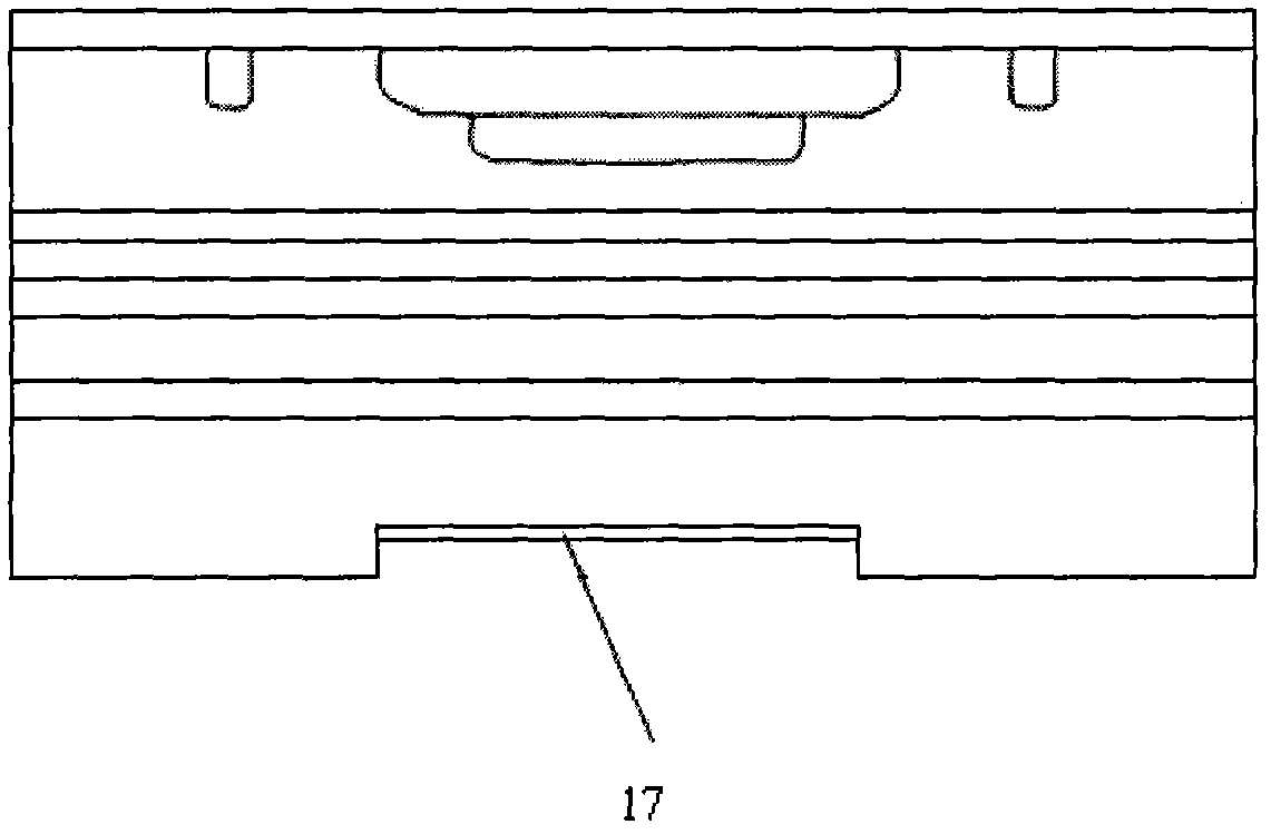
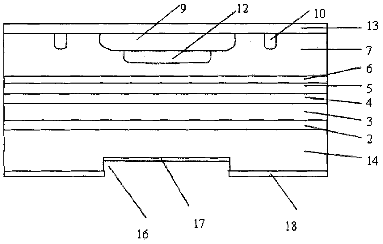
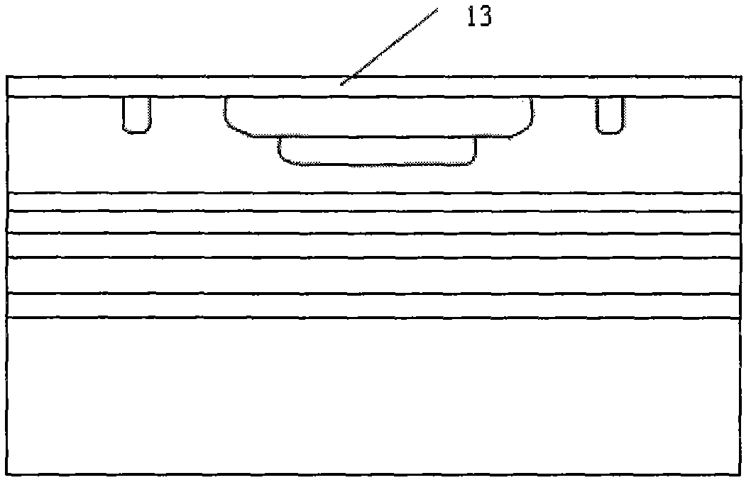
[0031] The invention adopts MOCVD epitaxy equipment to carry out primary epitaxy of avalanche photodiode on indium phosphide substrate, adopts MOCVD epitaxy equipment double-diffusion mode diffusion method to do doping and sputter P surface electrode, substrate is thinned, and light entrance hole on the back Wet etching, growing anti-reflection layer, making N-side electrode and electrode alloying.

[0032] The present invention will be described in detail below with reference to the accompanying drawings.

[0033] The primary epitaxy of the avalanche photodiode is carried out on the indium phosphide substrate by MOCVD, and the epitaxy is composed of seven layers (see figure 1 ), from bottom to top are S-doped N-type indium phosphide substrate 1, 1 micron N-type indium phosphide buffer layer 2, 2 micron doping concentration of i-type indium gallium arsenic absorber layer of 1E15cm^(-3) 3. 0.2 micron N-type indium phosphide layer 4, 0.12 micron InGaAsP gradient layer 5, 0.4 mi...


PUM


Abstract

The invention relates to a method for manufacturing a double diffusion type optical avalanche diode with incident light on a back surface by adopting epitaxial equipment. MOCVD epitaxial equipment is used for carrying out epitaxial treatment once on an avalanche photodiode on an indium phosphide substrate; a double diffusion method of the MOCVD epitaxial equipment is used for doping; a sputtering method is used for manufacturing a P-surface electrode; the substrate is thinned and polished; a wet corrosion method is used for manufacturing a light incidence window and an anti-reflection layer; the sputtering method is used for manufacturing a N-surface electrode; and the N-surface electrode is alloyed. By using the double diffusion method, in the diffusion process, the invention realizes gradient doping of different regions and different concentration by controlling the flow rate of a diffusion source; and an abrupt junction is formed in diffusion. The invention has good diffusion uniformity and high rate of finished products of pieces; and the manufactured avalanche photodiode with incident light on the back surface has the characteristics of small dark current, high sensitivity, small series resistance, high reliability and the like.

Description

technical field [0001] The invention relates to a method for manufacturing a high-sensitivity avalanche photodiode used in an optical communication system, in particular to a method for manufacturing a double-diffused back light incident optical avalanche tube using epitaxy equipment. Background technique [0002] The explosive growth of people's requirements for data services has promoted the rapid development of optical fiber communication technology. The development of optical fiber communication technology depends on the development level of optical fiber communication devices. Semiconductor photodetectors are the key components of the receiving part in optical fiber communication technology. Optical fiber communication technology is developing in the direction of high speed, large capacity and long distance. Avalanche photodiodes absorb incident photons by stimulated absorption to generate electron-hole pairs. There is a high electric field area in the avalanche photod...

Claims


Application Information

Patent Timeline
IPC IPC(8): H01L31/18H01L31/107
Inventor 秦龙吴瑞华唐琦
Owner WUHAN HUAGONG GENUINE OPTICS TECH
Why Eureka
Try Eureka