
Manufacturing method of inversed AlGaInP light emitting diode

A technology of aluminum gallium indium phosphide and light-emitting diodes, applied in semiconductor devices, electrical components, circuits, etc., can solve the problems of unstable process, complex process, and difficulty in accurately controlling the area of ​​the light-emitting area, so as to improve process stability and simplify The effect of craft

Active Publication Date: 2012-07-11
ANHUI SANAN OPTOELECTRONICS CO LTD
View PDF6 Cites 0 Cited by
  • Summary
  • Abstract
  • Description
  • Claims
  • Application Information

AI Technical Summary

Problems solved by technology

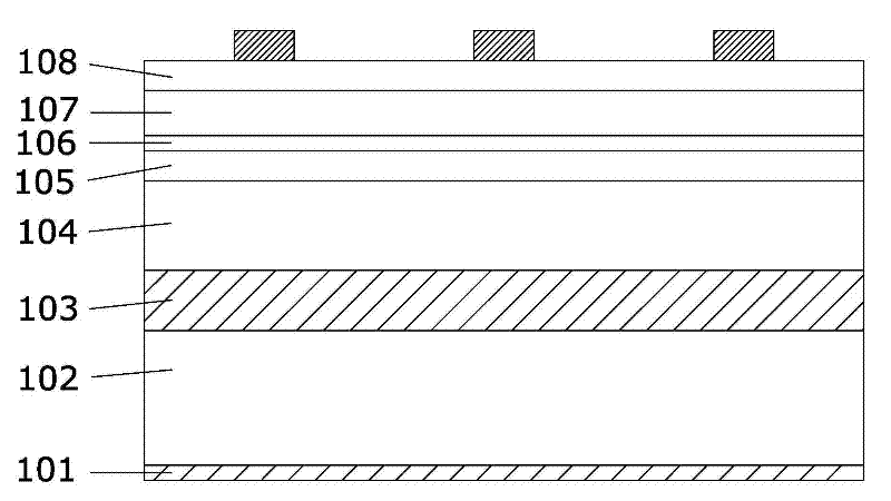
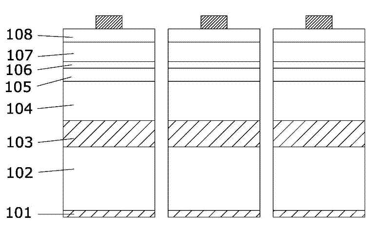
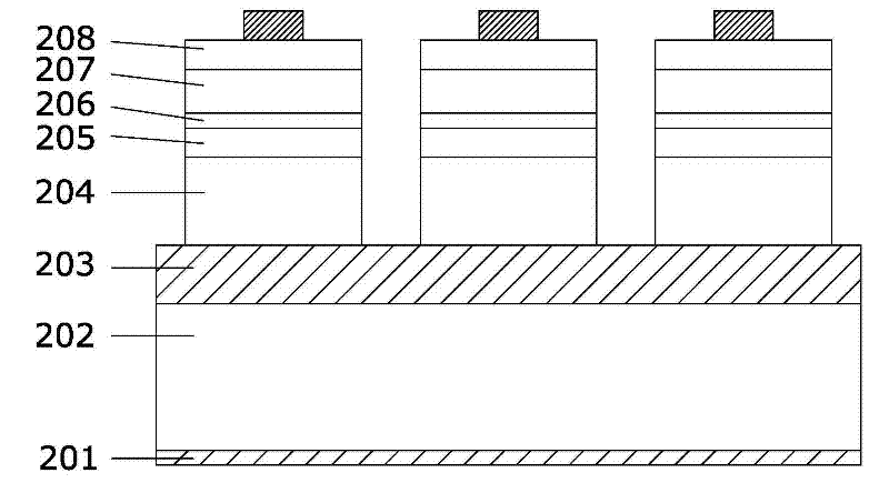
(Such as Figure 2b) The width of the cutting track is greater than the thickness of the diamond blade , the diamond knife will not touch the epitaxial layer during cutting, thereby avoiding bringing the metal layer 202 on the substrate 201 to the sidewalls of the epitaxial layers 207, 206, 205, 204 and 203, and avoiding serious electric leakage; However, dry etching will produce etching reactants that will adhere to the sidewall of the epitaxial layer and need to be removed by a solution; the solution will also etch the epitaxial layer when removing the product of dry etching, making the edge of the dicing line untidy, so it is difficult to accurately control The area of ​​the light-emitting area; therefore, the above-mentioned process is complicated, and it is difficult to strictly repeat the process in mass production, resulting in unstable process

Method used


Image

  • Manufacturing method of inversed AlGaInP light emitting diode
  • Manufacturing method of inversed AlGaInP light emitting diode
  • Manufacturing method of inversed AlGaInP light emitting diode

Examples


Embodiment Construction

[0025] The present invention will be further described below in conjunction with the accompanying drawings and embodiments.

[0026] A method for manufacturing a flip-chip aluminum gallium indium phosphide light-emitting diode, the process steps are as follows: Figure 3a As shown, GaAs buffer layer 302, GaInP cut-off layer 303, GaAs ohmic contact layer 304, n-AlGaInP confinement layer 305, The epitaxial light-emitting layer composed of multiple quantum well active layer 306, p-AlGaInP confinement layer 307 and p-GaP window layer 308; wherein: GaAs ohmic contact layer 304 is the second conductivity type ohmic contact layer, and n-AlGaInP confinement layer 305 is The second conductivity type confinement layer, the first conductivity type confinement layer is the p-AlGaInP confinement layer 307, the p-GaP window layer 308 is the first conductivity type window layer; SiO is grown on the p-GaP window layer 308 2 In the dielectric layer 309, the photomask defines the scribe line p...


PUM


Abstract

The invention discloses a manufacturing method of an inversed AlGaInP light emitting diode. A buffer layer, a cut-off layer, a second conduction-type ohm contact layer, a second conduction-type limiting layer, an active layer, a first conduction-type limiting layer and a first conduction-type window layer successively are subject to epitaxial growth on a temporary substrate to form an epitaxial luminescent layer; a media layer grows on the epitaxial luminescent layer, the graph of a cutting path is defined, and the media layer out of the cutting path is etched; the width of the media layer onthe cutting path is more than that of the tool edge of a diamante for cutting; a reflector is evaporated on the epitaxial luminescent layer; the back and the upper surface of a permanent substrate are respectively manufactured with a first ohm contact electrode and an evaporation bonding layer; the reflector is bonded with the bonding layer, and the temporary substrate, the buffer layer and the cut-off layer are removed; the second conduction-type ohm contact layer is manufactured with a second ohm contact electrode; and the obtained product is cut to obtain a chip. The invention solves the electric leakage problem brought by cutting, does not need to etch the epitaxial layer on the cutting path, simplifies the manufacturing technology and improves the technology stability.

Description

technical field [0001] The invention relates to a method for preparing a photoelectric semiconductor light-emitting device, in particular to a method for manufacturing an inverted aluminum gallium indium phosphide light-emitting diode. Background technique [0002] A light emitting diode (Light Emitting Diode, LED) is a luminescent light-emitting component. Its light-emitting principle is to apply a current to the III-V compound semiconductor material, and use the combination of electrons and holes in the diode to convert energy into the form of light. It glows when released, and won't get hot like an incandescent bulb after a long time of use. The advantages of light-emitting diodes are small size, long life, low driving voltage, fast response rate, and excellent shock resistance. product. [0003] Taking aluminum gallium indium phosphide (AlGaInP) light-emitting diodes as an example, aluminum gallium indium phosphide is a four-element compound semiconductor material, whi...

Claims


Application Information

Patent Timeline
Patent Type & Authority Patents(China)
IPC IPC(8): H01L33/00
Inventor 洪灵愿吴志强林素慧尹灵峰林潇雄
Owner ANHUI SANAN OPTOELECTRONICS CO LTD
Learn More