Passivation layer and its manufacturing method

A manufacturing method and passivation layer technology, applied in semiconductor/solid-state device manufacturing, electrical components, electrical solid-state devices, etc., can solve the problems of reducing the yield rate of semiconductor chips, poor adhesion, falling off, etc., to avoid peeling and Effects of cavitation, promotion of low temperature formation, and slowing down of migration

Inactive Publication Date: 2015-11-25
SHANGHAI INTEGRATED CIRCUIT RES & DEV CENT
View PDF5 Cites 0 Cited by
  • Summary
  • Abstract
  • Description
  • Claims
  • Application Information

AI Technical Summary

Problems solved by technology

Due to the difference in Young's modulus and thermal expansion coefficient of the silicon dioxide layer 20 and the silicon oxynitride layer 10, the silicon dioxide layer 20 and the silicon oxynitride layer 10 of the above-mentioned process all apply shrinkage stress to the metal line 30, so that the passivation The adhesion between the layer and the metal wire 30 becomes poor, and even the metal wire 30 will be pulled out, and then there will be voids, cracks or shedding between the metal wire 30 and the passivation layer, which reduces the quality of the semiconductor chip. Rate

Method used


Image

  • Passivation layer and its manufacturing method
  • Passivation layer and its manufacturing method

Examples


Embodiment Construction

[0023] Below in conjunction with accompanying drawing, the present invention is described in further detail:

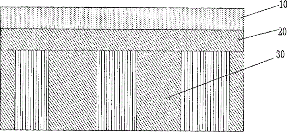
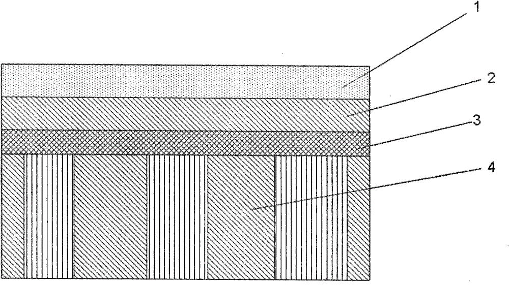
[0024] figure 2 In , the device layer of the semiconductor chip substrate is omitted, and the structure of the metal line and the passivation layer is only drawn schematically. Those skilled in the art can understand that a CMOS device can be pre-fabricated in the semiconductor substrate, and a metal line can be formed by using a dual embedded interconnection process.

[0025] Such as figure 2 As shown, the passivation layer of the present invention includes an amorphous silicon layer 3 formed on the semiconductor substrate and covering the metal line 4 in the semiconductor substrate, and formed sequentially on the amorphous silicon layer 3 Silicon dioxide layer 2 and silicon nitride layer 1. The metal wire 4 is copper wire. That is to say, the metal wire 4 of the semiconductor chip is made by copper wire technology.

[0026] The thickness of the amorphous sili...


PUM


Abstract

The invention discloses a passivation layer and a production method thereof. The passivation layer comprises an amorphous silicon layer (3), and a silicon dioxide layer (2) and a silicon oxynitride layer (1) which are formed on the amorphous silicon layer (3) in sequence, wherein the amorphous silicon layer (3) is formed on a semiconductor substrate and covers a metal wire (4) in the semiconductor substrate. The production method of the passivation layer comprises the following steps of: S01, depositing the amorphous silicon layer (3) on the semiconductor substrate, wherein the amorphous silicon layer (3) covers the semiconductor substrate and the metal wire (4) in the semiconductor substrate; S02, depositing the silicon dioxide layer (2) on the amorphous silicon layer (3); and S03, depositing the silicon oxynitride layer (1) on the silicon dioxide layer (2). The invention is applied to the technical field of semiconductor production and can enhance the yield rate of semiconductor chips.

Description

technical field [0001] The invention relates to the field of semiconductor chip manufacturing, in particular to a passivation layer formed on a semiconductor substrate and covering metal lines in the semiconductor substrate and a manufacturing method thereof. Background technique [0002] In the manufacturing process of semiconductor devices, the passivation of the device surface is one of the key technologies. Passivating the surface of the semiconductor device can reduce various charges in the oxide layer of the device, enhance the ability of the semiconductor chip to block ion contamination, protect the interconnection of the device inside the semiconductor chip and the electrical characteristics of the surface of the semiconductor chip, and prevent the semiconductor chip device from being damaged. mechanical and chemical damage. In the manufacturing process of semiconductor chip passivation layer, methods such as deposition and sputtering are often used. Due to the diff...

Claims


Application Information

Patent Timeline
Patent Type & Authority Patents(China)
IPC IPC(8): H01L23/29H01L23/31H01L21/56
Inventor 曾绍海张伟李铭
Owner SHANGHAI INTEGRATED CIRCUIT RES & DEV CENT
Why Eureka
Try Eureka