High-mobility quantum-dot field effect transistor and manufacturing method thereof

A field-effect transistor and high-mobility technology, which is applied in semiconductor/solid-state device manufacturing, semiconductor devices, electrical components, etc., can solve the problems of few studies on the influence of output characteristics, achieve practical and reliable methods, increase yield, reduce The effect of small degradation

Inactive Publication Date: 2011-03-30
INST OF SEMICONDUCTORS - CHINESE ACAD OF SCI
View PDF0 Cites 14 Cited by
  • Summary
  • Abstract
  • Description
  • Claims
  • Application Information

AI Technical Summary

Problems solved by technology

[0004] Since the S-K mode growth technology has matured, people have conducted extensive research on the influence of the charge and discharge of the obtained quantum dots and the potential energy change caused by the process on the electrical transport properties. In terms of the influence of the two-dimensional electron gas (2DEG), but there are few studies on the influence of the interaction between the two-dimensional electron gas layer and the quantum dot layer on the output characteristics.

Method used


Image

  • High-mobility quantum-dot field effect transistor and manufacturing method thereof
  • High-mobility quantum-dot field effect transistor and manufacturing method thereof
  • High-mobility quantum-dot field effect transistor and manufacturing method thereof

Examples


Embodiment Construction

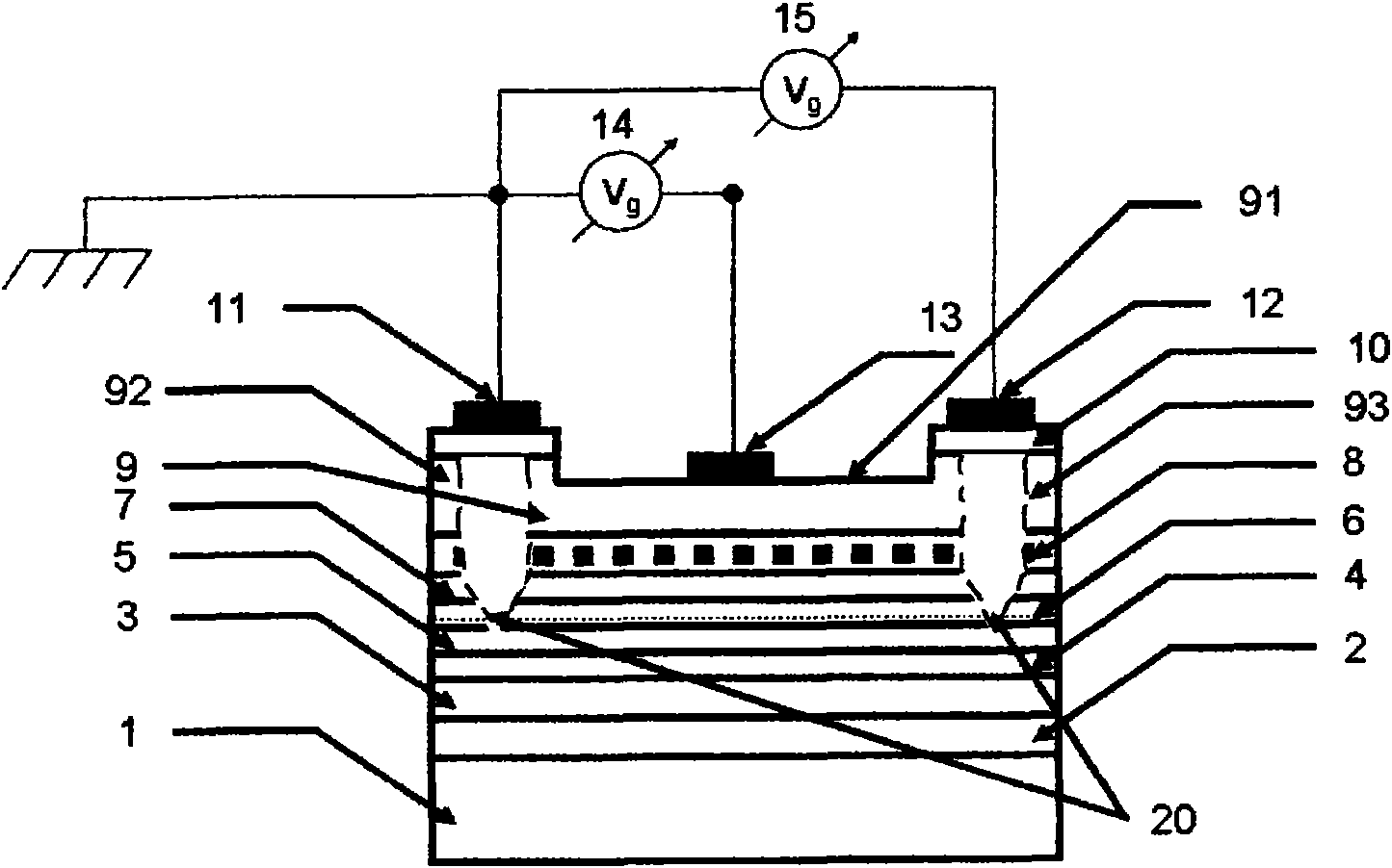
[0042] see figure 1 Shown, a kind of high mobility quantum dot field effect transistor of the present invention comprises:

[0043] A substrate 1, the substrate 1 is a semi-insulating gallium arsenide or indium phosphide substrate of the (100) plane, to provide the required crystal plane for anisotropic etching and reduce the leakage current of the substrate;

[0044] A first stress buffer layer 2, the first stress buffer layer 2 is fabricated on the substrate 1;

[0045] A second stress buffer layer 3, the second stress buffer layer 3 is made on the first stress buffer layer 2, the stress buffer layer 2 and the stress buffer layer 3 are undoped semiconductor materials, the purpose is to obtain high-quality epitaxy Layer, to reduce the influence of defects in the substrate on the electron channel layer 6, the thickness needs to be more than 100nm, and a thicker stress buffer layer will have a better effect, but the cost will increase accordingly. Generally, GaAs with a total ...


PUM


Abstract

The invention discloses a high-mobility quantum-dot field effect transistor which comprises a substrate, a first stress buffer layer, a second stress buffer layer, a doping layer, a spacer layer, a channel layer, a lower potential barrier layer, a quantum-dot layer, an upper potential barrier layer, two cap layers, a first electrode, a second electrode and a third electrode, wherein the first stress buffer layer is manufactured on the substrate; the second stress buffer layer is manufactured on the first stress buffer layer; the doping layer is manufactured on the second stress buffer layer; the spacer layer is manufactured on the doping layer; the channel layer is manufactured on the spacer layer; the lower potential barrier layer is manufactured on the channel layer; the quantum-dot layer is manufactured on the lower potential barrier layer; the upper potential barrier layer is manufactured on the quantum-dot layer, a concave mesa is arranged on the middle of the top of the upper potential barrier layer, one side of the concave mesa is provided with a source region, and the other side of the concave mesa is provided with a drain region; the two cap layers are respectively manufactured on the source region and the drain region which are at the two sides of the upper potential barrier layer; the first electrode is manufactured on the top of one cap layer; the second electrode is manufactured on the top of the other cap layer; and the third electrode is manufactured on the concave mesa on the top of the upper potential barrier layer.

Description

technical field [0001] The invention relates to the field of semiconductor materials and devices, in particular to a high mobility quantum dot field effect transistor. Background technique [0002] Confinement nanostructures such as quantum dots and quantum wires are a hotspot in the research of solid state physics and device engineering. Among them, quantum dots with zero-dimensional electron / hole confinement have attracted extensive attention because of their important roles in both physics and device fields. Its application prospects include nonlinear transmission, improving the performance of lasers and detectors, realizing high-density semiconductor memory, etc. [0003] At present, the most promising preparation method to realize 10nm quantum dots with high density and high uniformity is the Stranski-Krastanov (S-K) epitaxial growth mode. In this method, a material is deposited on a lattice-mismatched substrate. When the thickness of the epitaxial material exceeds a ...

Claims


Application Information

Patent Timeline
Patent Type & Authority Applications(China)
IPC IPC(8): H01L29/778H01L21/335H01L21/78
Inventor 李越强刘雯王晓东陈燕玲杨富华
Owner INST OF SEMICONDUCTORS - CHINESE ACAD OF SCI
Why Eureka
Try Eureka