Wafer level chip size packaging structure and manufacturing method thereof

A wafer-level chip and size packaging technology, which is applied in semiconductor/solid-state device manufacturing, electrical components, electric solid-state devices, etc., can solve the problems of unfavorable chip cost reduction, complex packaging structure, and long production cycle, so as to increase market competition Capability, simple and easy manufacturing method, and cost-saving effect

Active Publication Date: 2011-04-13
SEMICON MFG INT (SHANGHAI) CORP
View PDF0 Cites 6 Cited by
  • Summary
  • Abstract
  • Description
  • Claims
  • Application Information

AI Technical Summary

Problems solved by technology

[0023] In order to solve the complex structure and long production cycle of wafer-level chip size packaging in the prior art, the existing manufacturing method of wafer-level chip size packaging structure has complicated steps, high cost, and long production cycle, ...

Method used


Image

  • Wafer level chip size packaging structure and manufacturing method thereof
  • Wafer level chip size packaging structure and manufacturing method thereof
  • Wafer level chip size packaging structure and manufacturing method thereof

Examples


Embodiment 1

[0058] Figure 2A to Figure 2DIt is a schematic diagram of each step of the manufacturing method of the WLCSP structure according to an embodiment of the present invention.

[0059] The manufacturing method of the wafer-level chip size packaging structure of this embodiment includes:

[0060] Firstly, a wafer is provided, the wafer has pads thereon;

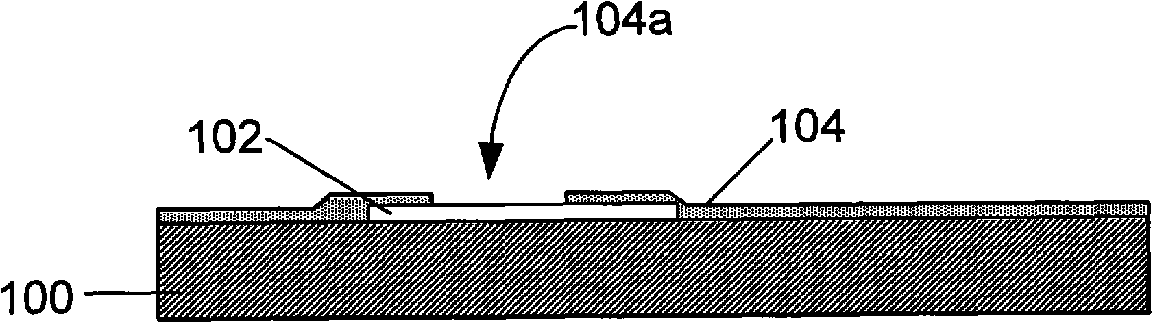
[0061] Such as Figure 2A As shown, the wafer includes: a substrate 200, a pad 202 located on the substrate 200, and a substrate passivation layer 204 partially covering the pad 202, and the substrate passivation layer 204 has an exposed portion The substrate passivation layer through hole 204a of the pad 202; wherein the material of the substrate 200 is silicon, and the material of the pad is aluminum; the substrate passivation layer 204 can be made of epoxy polymer ;

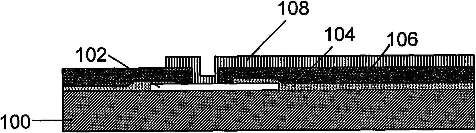
[0062] Secondly, the optical process of the redistribution layer 208 is performed;

[0063] Preferably, the material of the rewiring layer 108 is copper (Cu...

Embodiment 2

[0080] This embodiment illustrates another preferred method for manufacturing a wafer-level chip-scale package structure, including:

[0081] Step 1: provide the wafer;

[0082] The wafer includes: a substrate 200, a pad 202 located on the substrate 200, and a substrate passivation layer 204 partially covering the pad 202, and the substrate passivation layer on the pad 202 204 has a substrate passivation layer through hole 204a to expose part of the pad 202; wherein the material of the substrate 200 is silicon, and the material of the pad is aluminum;

[0083] Step 2: Preprocessing the wafer;

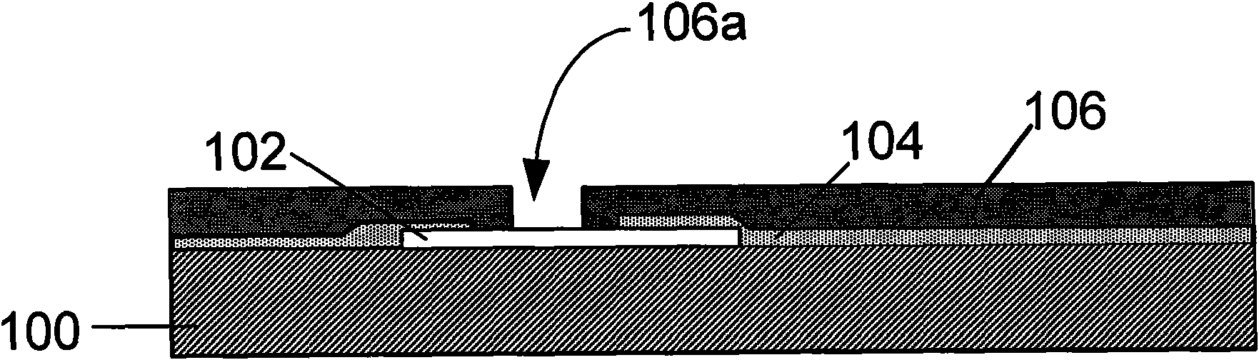
[0084] Step 3: performing photo-processing of the first passivation layer 206 on the wafer;

[0085] The first passivation layer 206 can be polyimide (PI), poly-p-phenylene benzobisoxazole (PBO) or photosensitive benzocyclobutene, and the photo process can be yellow light process;

[0086] Step 4: Etching the first passivation layer 206 to form a first passivation layer through hole ...


PUM

PropertyMeasurementUnit
Thicknessaaaaaaaaaa

Abstract

The invention provides a manufacturing method of a wafer level chip size packaging structure, which comprises the following steps of: providing a wafer, and arranging a welding pad on the wafer; performing the photo processing of a rewiring layer on the wafer; forming and etching the rewiring layer so as to form a required pattern, wherein the rewiring layer is electrically connected with the welding pad; performing the photo processing of a second passivation layer on the wafer; etching the second passivation layer to form a through hole of the second passivation layer so as to expose the rewiring layer, curing the second passivation layer and removing scum; implanting a welded ball in the through hole of the second passivation layer, wherein the welded ball and the rewiring layer are electrically connected; and inspecting the quality of the wafer before product delivery. The invention also provides the wafer level chip size packaging structure manufactured according to the manufacturing method. The manufacturing method of the invention saves processing steps and materials and reduces the cost and the competitiveness of the product.

Description

technical field [0001] The invention relates to the field of semiconductor device manufacturing, in particular to a wafer-level chip size packaging structure and a manufacturing method thereof. Background technique [0002] Wafer Level Chip Size Packaging (WLCSP, Wafer Level Chip Size Packaging) technology is a technology for packaging and testing the entire wafer and then cutting it to obtain individual chips. Generally, the wafer-level chip size package is to distribute the pads (Pads) arranged on the periphery of the semiconductor chip into a large number of solder balls in an area array through a redistribution process, or the solder balls are called solder bumps. [0003] Since the chip size after wafer-level chip size packaging has reached a high degree of miniaturization, the cost of the chip is significantly reduced with the reduction of chip size and the increase of wafer size. Therefore, wafer-level chip size packaging is the current packaging field. hotspots and ...

Claims


Application Information

Patent Timeline
IPC IPC(8): H01L21/50H01L21/60H01L23/485H01L23/488H01L23/482
CPCH01L24/11H01L2224/11H01L2924/00012
Inventor 梅娜佟大明
Owner SEMICON MFG INT (SHANGHAI) CORP
Why Eureka
Try Eureka