Film deposition method

A thin film deposition, anode plate technology, applied in gaseous chemical plating, metal material coating process, coating and other directions, can solve the problem of large gas flow, large gas consumption, film consistency and thickness uniformity decline, etc. It can solve the problem of uniformity, save the reaction gas, and reduce the probability of pollution.

Inactive Publication Date: 2011-04-20
APOLLO PRECISION (FUJIAN) LIMITED
View PDF3 Cites 2 Cited by
  • Summary
  • Abstract
  • Description
  • Claims
  • Application Information

AI Technical Summary

Problems solved by technology

[0006] Although the PECVD process has the characteristics of simple process and high deposition efficiency, it is difficult to obtain large-area substrates (for example, with an area greater than 0.7m 2 ) when depositing a large area of ​​nanocrystalline silicon film on the surface, the consistency and thickness uniformity of the film layer will be significantly reduced
In addition, the traditional PECVD process is to provide reaction gas (usually a source gas mixture of silane and hydrogen) to the reaction chamber from the outside, and the reaction gas is in the reaction chamber, especially a large reaction chamber for large-area substrate deposition (for example, the patent No. The distribution uniformity in the large-scale PECVD deposition equipment described in the Chinese patent of 200820008274.5 is difficult to guarantee, and it is easy to cause impurity pollution, which affects the uniformity and consistency of the nanocrystalline silicon film
In addition, the electrode structure of traditional PECVD equipment is complex, and in order to obtain a high deposition rate and a suitable degree of crystallization, a large gas flow rate is required, and the gas consumption is large
The complexity of equipment and high consumption of raw materials increase production costs and significantly reduce product competitiveness

Method used


Image

  • Film deposition method
  • Film deposition method
  • Film deposition method

Examples


Embodiment Construction

[0037] In order to make the above objects, features and advantages of the present invention more comprehensible, specific implementations of the present invention will be described in detail below in conjunction with the accompanying drawings. In the following description, numerous specific details are set forth in order to provide a thorough understanding of the present invention. However, the present invention can be implemented in many ways other than those described here, and those skilled in the art can make similar extensions without departing from the connotation of the present invention. Accordingly, the invention is not limited to the specific implementations disclosed below.

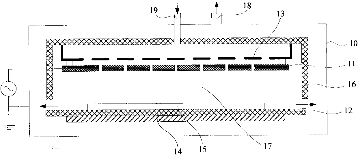
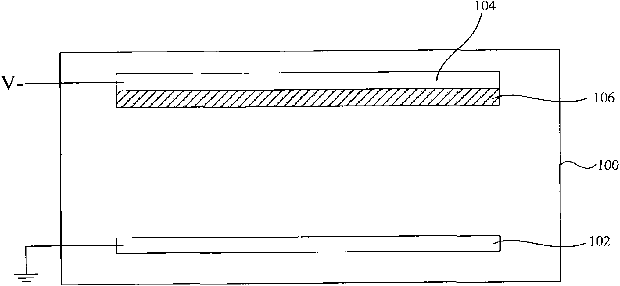
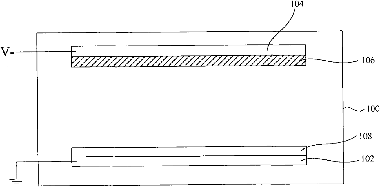
[0038] The following takes the deposition of silicon-based thin films as an example, combining Figure 2 to Figure 6The thin film deposition method of the present invention will be described in detail. According to the embodiment of the present invention, the silicon film is deposited on the ...


PUM


Abstract

The invention discloses a film deposition method, which comprises the following steps of: oppositely placing an anode plate and a cathode plate in parallel in a reaction chamber, wherein the surface of the cathode plate, which faces to the anode plate, is provided with a sacrifice layer; placing a conducted base plate or a base plate with a conduction layer on which the conduction layer contacts the surface of the anode plate on the surface of the anode plate, which faces to the sacrifice layer; introducing hydrogen; and building a direct-current electric field between the anode plate and the cathode plate, exciting the hydrogen into a plasma and etching the sacrifice layer, and depositing a film which is based mainly on sacrifice layer substances on the surface of the base plate. By using the method, raw material gas including film substances does not need providing from outside, and the direct-current electric field is used for excitation, which greatly simplifies equipment and process for manufacturing large-area microcrystalline silicon photoelectric devices.

Description

technical field [0001] The invention relates to the technical field of photovoltaic solar cells, in particular to a thin film deposition method. Background technique [0002] With the increasing shortage of energy, the development and utilization of renewable green energy has attracted more and more attention, especially the utilization of solar energy has attracted the attention of the world. As a solar energy conversion medium, solar cells, especially the silicon-based thin-film solar cells that have emerged in recent years, represent the development trend of photovoltaic technology with their advantages of large area, low cost, deposition on light and thin substrates, and easy laying and installation. [0003] Thin-film solar cells are used to convert light energy emitted by light sources such as sunlight, lamps or fluorescent lights into electrical energy. This conversion is generated by the photovoltaic (photoelectric) effect of semiconductor materials. When light irrad...

Claims


Application Information

Patent Timeline
Patent Type & Authority Applications(China)
IPC IPC(8): C23C16/503C23C16/455
Inventor 李沅民王树林张迎春
Owner APOLLO PRECISION (FUJIAN) LIMITED
Why Eureka
Try Eureka