Method for selectively depositing thin film on substrate by utilizing atomic layer deposition

An atomic layer deposition, selective technology, used in coatings, metal material coating processes, gaseous chemical plating, etc.

Inactive Publication Date: 2011-04-27
FUDAN UNIV
View PDF0 Cites 5 Cited by
  • Summary
  • Abstract
  • Description
  • Claims
  • Application Information

AI Technical Summary

Problems solved by technology

[0007] The shortcomings of the above growth processes have brought great prob...

Method used


Image

  • Method for selectively depositing thin film on substrate by utilizing atomic layer deposition
  • Method for selectively depositing thin film on substrate by utilizing atomic layer deposition
  • Method for selectively depositing thin film on substrate by utilizing atomic layer deposition

Examples


Embodiment 1

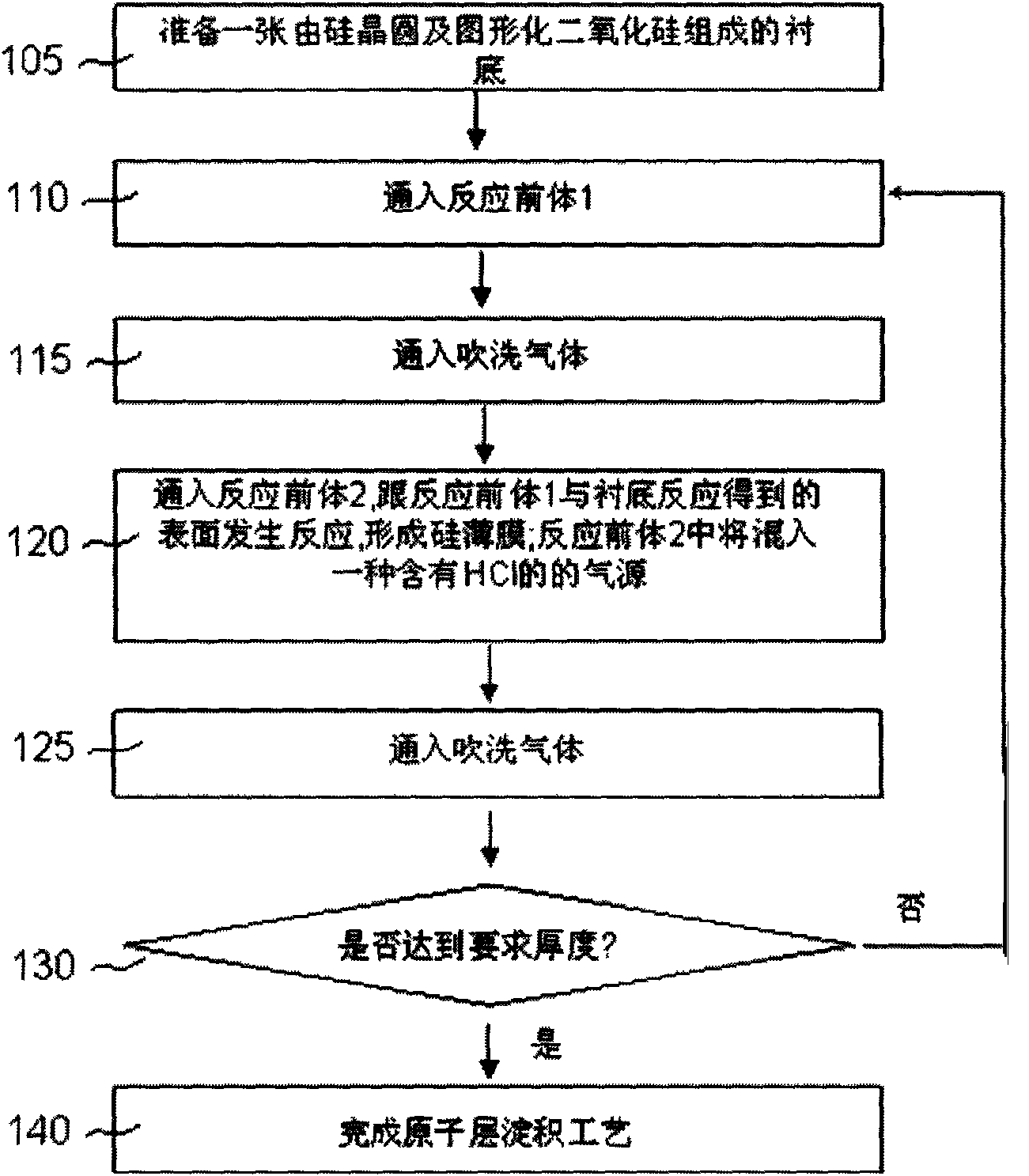
[0032] figure 1 It is a process flow diagram of selective deposition of silicon and germanium by atomic layer deposition. The oxides mentioned in the figure can be replaced by nitrides in some applications. First, the substrate is placed in the ALD reaction chamber. At 110, a silicon-containing reactive precursor, such as SiH2Cl2 or SiCl4, is introduced at the substrate. SiH2Cl2 or SiCl4 will be adsorbed on the substrate surface. Then, at 115, a purge gas is introduced into the reaction chamber. Nitrogen, argon or other inert gases can be used as purge gas. At 120, a second reactive precursor is passed into the reaction chamber. This reactive precursor can be SiH4 or GeH4. The second reaction precursor reacts with the Si-Cl group or other groups formed on the surface of the first reaction precursor to form HCl and the silicon or silicon germanium film we need. exist figure 1 In , selective deposition is achieved by mixing HCl gas in the second reactive precursor. HCl ...

Embodiment 2

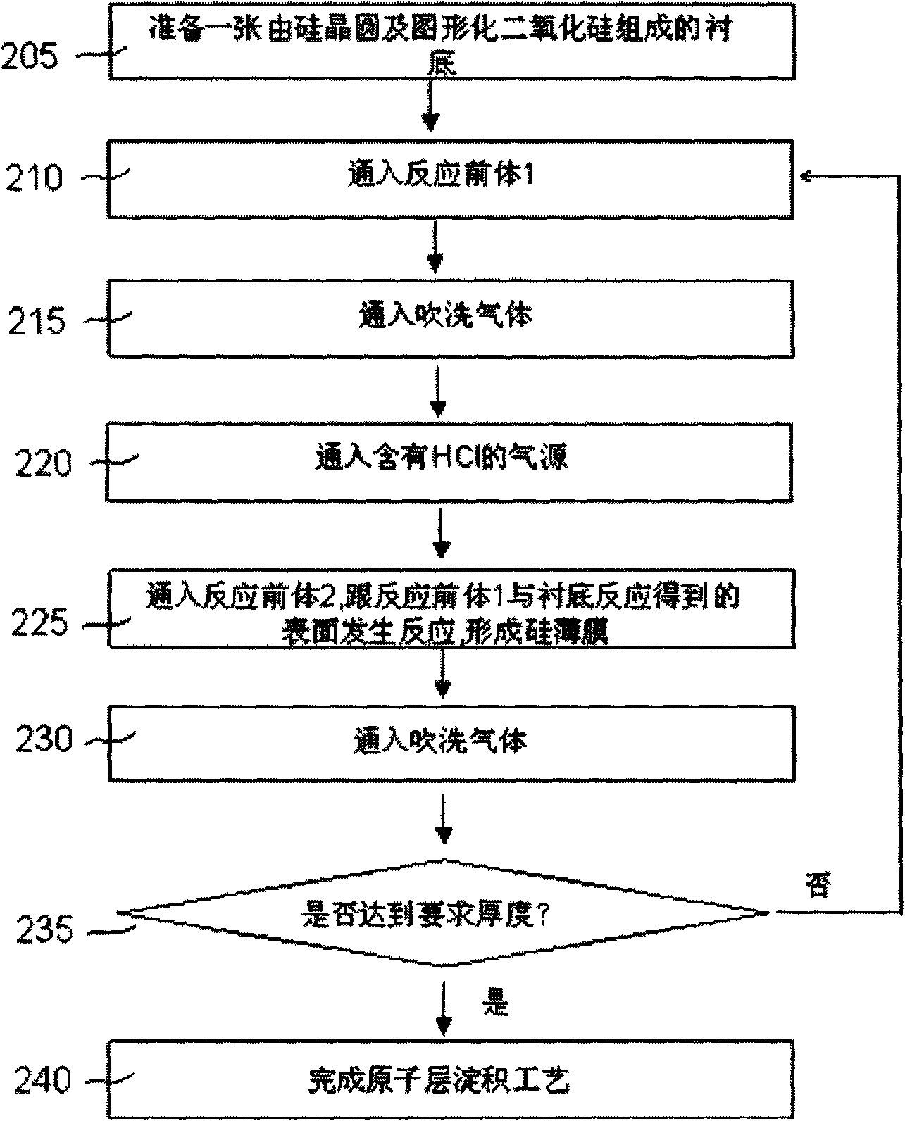
[0035] figure 2 It is the process flow diagram of the second selective deposition of silicon and germanium by atomic layer deposition.

[0036] First, with figure 1 Similar to the above, the process flow starts from 205, that is, a substrate including a semiconductor wafer and a patterned oxide. In some applications, the oxides can be replaced by nitrides. Treated substrates with figure 1 In the same way, it is placed in the atomic layer reaction chamber. At 210, silicon-containing reactive precursors, such as SiH2Cl2 and SiCl4, are passed into the reaction chamber to reach the substrate surface. SiH2Cl2 and SiCl4 will be adsorbed on the substrate surface. Then, at 215, a purge gas is introduced into the reaction chamber. Nitrogen, argon or other inert gases can be used as purge gas. follow Figure 1 The difference in is that figure 2 In , the HCl gas is not introduced into the reaction chamber together with the reaction precursor 2, but the introduction of HCl is r...

Embodiment 3

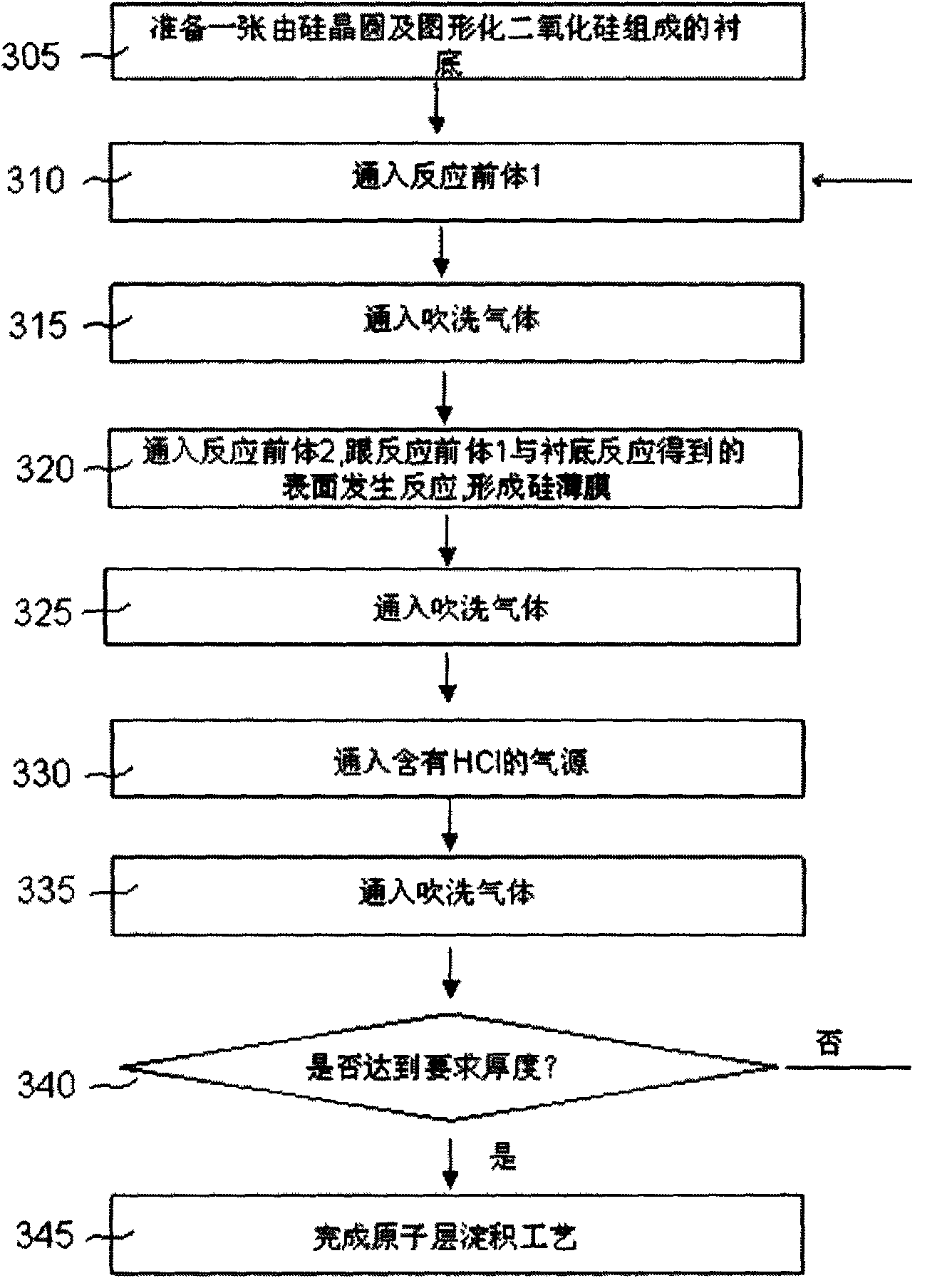
[0038] image 3 It is the process flow diagram of the third selective deposition of silicon and germanium by atomic layer deposition. like figure 1 In , the process flow starts from 305, a substrate including a semiconductor wafer and patterned oxide. In some applications, the oxide inside can be replaced by a nitride. Treated substrates with figure 1 It is placed in the atomic layer reaction chamber as in the process. At 310, silicon-containing reactive precursors, such as SiH2Cl2 and SiCl4, are passed into the reaction chamber to reach the substrate surface. SiH2Cl2 and SiCl4 will be adsorbed on the substrate surface. Then, at 315, a purge gas is introduced into the reaction chamber. Nitrogen, argon or other inert gases can be used as purge gas. At 320, a second reactive precursor is passed into the reaction chamber. This reaction precursor can be SiH4 or SiH2Cl2. The second reaction precursor reacts with the Si-Cl group or other groups formed on the surface of the ...


PUM


Abstract

The invention relates to a thin film deposition technology for preparing semiconductor devices, in particular to a method for selectively growing silicon, germanium silicon and derivative thin films thereof on a substrate by utilizing an atomic layer deposition technology. The substrate is heated to the preset temperature during the growth process against the substrate comprising a semiconductor wafer and oxide thin films with different density patterns, the atomic layer deposition method is utilized for growing the thin film on the surface of the substrate, and the effect of inhibiting the growth of the thin film on an oxide layer can be realized by doping HCl (hydrochloric acid) in a reaction precursor of the atomic layer deposition or independently introducing pulses of the HCl in the technological process. The thin film is deposited in a selected region and does not need to be deposited in other unnecessary places; by utilizing the method, the traditional selective deposition and growth way of depositing the thin film with load effect on the surfaces with the different density patterns can be solved; and the traditional lithography technology is not required, and the need of introducing the follow-up thin film etching process due to the use of the traditional lithography technology can be also omitted.

Description

technical field [0001] The invention relates to a thin film deposition technology for semiconductor device preparation. Specifically relates to a method for selective atomic layer deposition of thin films on a substrate Background technique [0002] Advanced thin film preparation technology is one of the key technologies for the scaling down of semiconductor devices. The proportional reduction of semiconductor devices is not only the reduction of traditional device structures, but also the introduction of new materials and device structures at the technology node of each integrated circuit. Through the above two points, the improvement of device performance at each technology node predicted according to Moore's Law can be maintained. [0003] Commonly used techniques for preparing thin films include sputtering, chemical vapor deposition, sol-gel method, physical vapor deposition, organic metal source chemical vapor deposition, and atomic layer deposition. Atomic layer dep...

Claims


Application Information

Patent Timeline
IPC IPC(8): C23C16/455C23C16/04H01L21/205
Inventor 吴东平孙清清张世理
Owner FUDAN UNIV
Why Eureka
Try Eureka