Method for preparing sequentially arranged bent silicon nano-wire array

A silicon nanowire array, orderly arrangement technology, applied in nanostructure manufacturing, nanotechnology, nanotechnology and other directions, to achieve the effect of mild reaction conditions and simple methods

Inactive Publication Date: 2011-05-04
TECHNICAL INST OF PHYSICS & CHEMISTRY - CHINESE ACAD OF SCI
View PDF2 Cites 23 Cited by
  • Summary
  • Abstract
  • Description
  • Claims
  • Application Information

AI Technical Summary

Problems solved by technology

However, there is no report on the preparatio

Method used


Image

  • Method for preparing sequentially arranged bent silicon nano-wire array
  • Method for preparing sequentially arranged bent silicon nano-wire array
  • Method for preparing sequentially arranged bent silicon nano-wire array

Examples


Embodiment 1

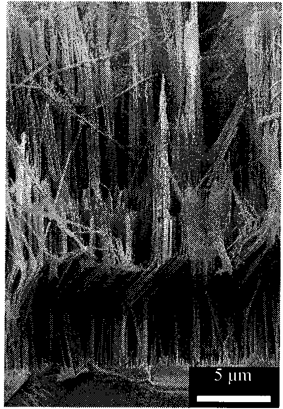
[0034] Example 1. Preparation of ordered array of bent silicon nanowires

[0035] The single crystal silicon wafer with a specific crystal orientation used in this embodiment is an N-type crystal orientation silicon wafer purchased from Tianjin Semiconductor Research Institute, with a resistivity of 0.015 ohm cm and a polished surface (mirror surface). In the experiment, silver nitrate, hydrofluoric acid aqueous solution (mass concentration is 40%) and deionized water are used to prepare an etching solution containing hydrofluoric acid concentration of 4.6mol / L and silver ion concentration of 0.04mol / L, and adding it to poly In a tetrafluoroethylene container; take an N-type crystalline silicon wafer, soak it in a chromic acid wash solution (prepared from 5 grams of potassium dichromate, 100 ml of concentrated sulfuric acid, and 10 ml of water) to remove organic pollutants on the surface of the silicon wafer, Then, it was treated with 10% hydrofluoric acid aqueous solution f...

Embodiment 2

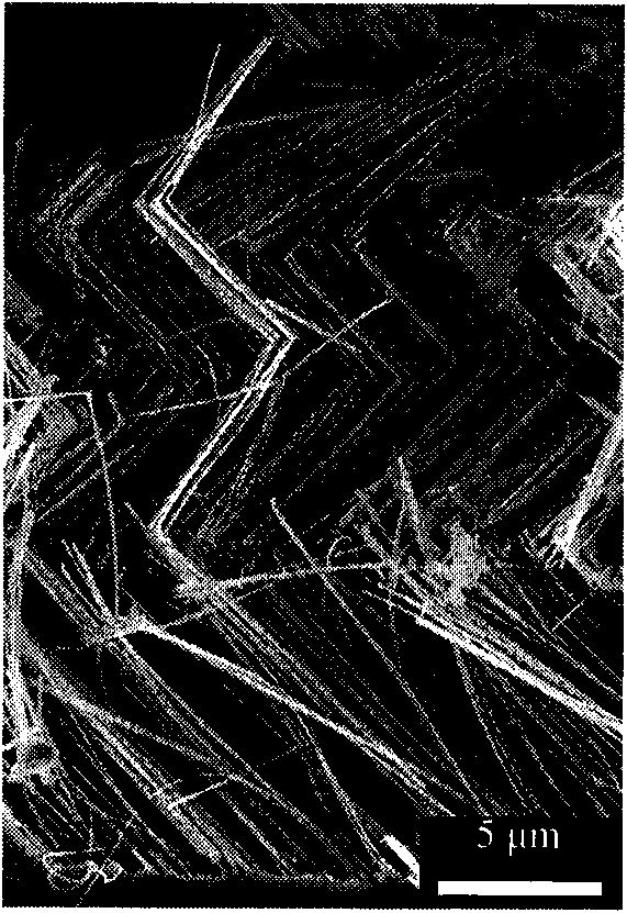
[0036] Example 2, Preparation of Orderly Arranged Bending Silicon Nanowire Arrays

[0037] According to the method of Example 1, the orderly arranged bent silicon nanowire array material is prepared, the difference is that the single crystal silicon wafer with a specific crystal orientation used in this example is a P-type crystal orientation silicon wafer (resistance Ratio: 0.015 ohm·cm), indicating that the method for preparing ordered arrays of bent silicon nanowires of the present invention has universal applicability. Observing the cross-sectional morphology of the silicon wafer under a scanning electron microscope, the obtained ordered array of bent silicon nanowires is as follows: figure 2 shown.

Embodiment 3

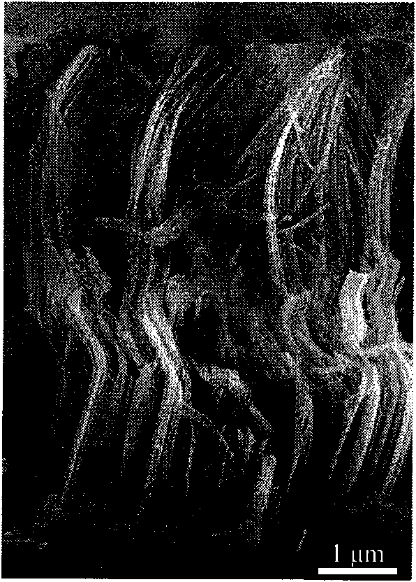
[0038] Example 3, Preparation of Orderly Arranged Bending Silicon Nanowire Arrays

[0039] According to the method of Example 1, the orderly arranged bent silicon nanowire array material is prepared, the difference is that the concentration of silver ions in the etching solution used in this example is 0.01mol / L, and the temperature used is 55 degrees Celsius. The obtained ordered array of bent silicon nanowires is as follows: image 3 shown.


PUM


Abstract

The invention discloses a method for preparing a sequentially arranged bent silicon nano-wire array. The method comprises the following steps of: 1) placing etching solution in a hydrofluoric acid corrosion resistant vessel, cleaning a crystal orientation mono-crystalline silicon wafer (111), immersing in the etching solution, and sealing the vessel, wherein the etching solution consists of silver nitrate, hydrofluoric acid and deionized water, the concentration of silver ions in the etching solution is between 0.01 and 0.04mol/L, and the concentration of the hydrofluoric acid is between 1 and 5mol/L; and 2) placing the vessel in a constant-temperature water bath to ensure the silicon wafer reacts with the etching solution, and taking the silicon wafer out after the reaction is completed to obtain the sequentially arranged bent silicon nano-wire array on the surface of the silicon wafer. In the method, the metal ion assisted solution etching technology and selective effect of different crystal orientations of the silicon wafer are organically combined so as to prepare the sequentially arranged bent silicon nano-wire array on the surface of the silicon wafer. The method is simple and convenient and has mild reaction conditions, and by the method, the sequentially arranged bent silicon nano-wire array material can be prepared in one step at room temperature.

Description

technical field [0001] The invention relates to a method for preparing an orderly arranged bent silicon nanowire array. Background technique [0002] Silicon nanostructure materials have special optical and electrical properties, and are widely used in optoelectronic devices and sensor devices. In order to facilitate the preparation and application of functional devices based on silicon nanostructures, it is very necessary to controlly introduce silicon nanostructures on the surface of silicon wafers through a specific process. [0003] In order to prepare silicon nanostructure materials on the surface of silicon wafers, there are reports in the literature on the application of electrochemical corrosion methods (L.T.Canham, Appl.Phys.Lett.1990, 57, 1046; S.Q.Li, T.L.S.L.Wijesinghe, D.J.Blackwood, Adv.Mater.2008, 20, 3165), but the electrochemical corrosion method is mainly used in the preparation of disordered silicon nanostructures such as porous silicon, and it is still d...

Claims


Application Information

Patent Timeline
IPC IPC(8): B82B3/00C01B33/021C23F1/24
Inventor 张晓宏陈欢王辉欧雪梅李述汤
Owner TECHNICAL INST OF PHYSICS & CHEMISTRY - CHINESE ACAD OF SCI
Why Eureka
Try Eureka