
Silicon-based double-junction solar cell with homojunction and heterojunction and preparation method thereof

A solar cell and homojunction technology, applied in circuits, photovoltaic power generation, electrical components, etc., can solve problems such as high manufacturing costs, high requirements for process parameter control, and attenuation of battery efficiency, and achieve cost-effective and simple process effects

Active Publication Date: 2011-05-18
ZHEJIANG JINGSHENG MECHANICAL & ELECTRICAL
View PDF5 Cites 17 Cited by
  • Summary
  • Abstract
  • Description
  • Claims
  • Application Information

AI Technical Summary

Problems solved by technology

The main problem is that the photoelectric efficiency is only slightly higher than that of ordinary diffused crystalline silicon solar cells, and in order to make the photoelectric performance consistent, the process parameter control requirements are relatively high, especially the thickness of the amorphous silicon layer must be strictly controlled, otherwise it may still cause cell efficiency. attenuation
[0008] In addition, there are some battery structures that can achieve greater than 20% efficiency, such as the buried groove solar cell (BCSC) developed by the University of New South Wales in Australia, the emitter passivation and the backside local diffusion solar cell (PERL), and the interdigitated solar cell. Back-contact electrode solar cells (IBC), etc., but these cells have complex structures and processes, and the manufacturing cost is too high compared with conventional cells

Method used


Image

  • Silicon-based double-junction solar cell with homojunction and heterojunction and preparation method thereof
  • Silicon-based double-junction solar cell with homojunction and heterojunction and preparation method thereof
  • Silicon-based double-junction solar cell with homojunction and heterojunction and preparation method thereof

Examples


Embodiment 1

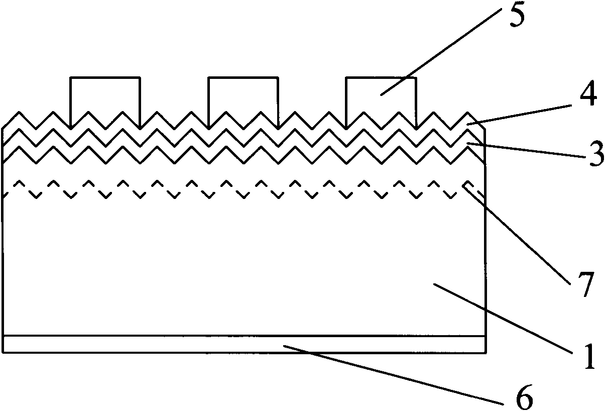
[0036] Such as figure 1 The front side of the P-type polysilicon wafer shown is a double-junction battery with a PN junction. The double-junction battery includes a P-type polysilicon wafer. The front side of the P-type polysilicon wafer forms a homogeneous PN junction. + type amorphous silicon film, N + An ITO transparent conductive film is arranged on the top of the non-crystalline silicon film, and a front metal electrode and a back metal electrode are respectively arranged on the top of the ITO transparent conductive film and the back of the polycrystalline silicon wafer.

[0037] figure 1 The reference signs in are as follows: 1, P-type polysilicon chip, 3, N + Type amorphous silicon film, 4. ITO transparent conductive film, 5. Front metal electrode, 6. Back metal electrode, 7. Homogeneous PN junction.

[0038] The preparation process of the above-mentioned double-junction cell with a PN junction on the front side of the P-type polysilicon wafer is as follows:

[00...

Embodiment 2

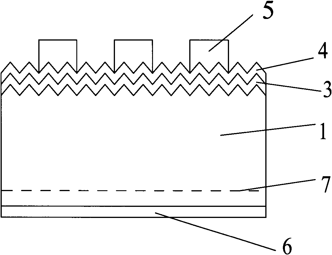
[0043] Such as figure 2 The back of the P-type single crystal silicon wafer shown is a double-junction battery with a PN junction. The double-junction battery includes a P-type single crystal silicon wafer. The upper side of the sheet is provided with a P + type amorphous silicon film, P + An ITO transparent conductive film is arranged on the top of the amorphous silicon film, and a front metal electrode and a back metal electrode are respectively arranged on the top of the ITO transparent conductive film and the back of the single crystal silicon wafer.

[0044] figure 2 The reference signs in are as follows: 1, P-type monocrystalline silicon wafer, 3, P + Type amorphous silicon film, 4. ITO transparent conductive film, 5. Front metal electrode, 6. Back metal electrode, 7. Homogeneous PN junction.

[0045] The preparation process of the above-mentioned double-junction cell with a PN junction on the back side of the P-type single crystal silicon wafer is as follows:

[...

Embodiment 3

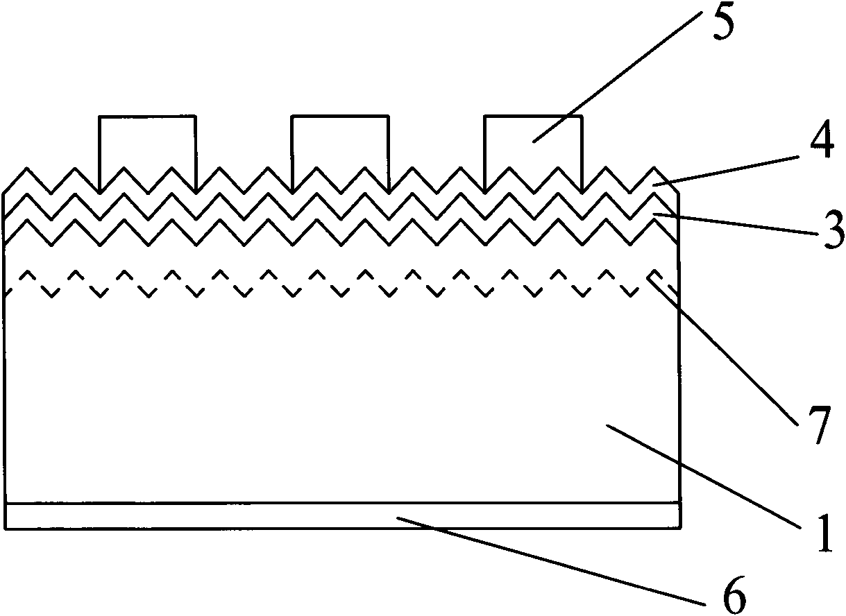
[0050] Such as image 3 The front side of the N-type single crystal silicon wafer shown is a double-junction battery with a PN junction. The double-junction battery includes an N-type single crystal silicon wafer. The front of the N-type single crystal silicon wafer forms a homogeneous PN junction. There is a P on the top of the front + type amorphous silicon film, P + An ITO transparent conductive film is arranged on the top of the amorphous silicon film, and a front metal electrode and a back metal electrode are respectively arranged on the top of the ITO transparent conductive film and the back of the single crystal silicon wafer.

[0051] image 3 The reference signs in are as follows: 1, N-type monocrystalline silicon wafer, 3, P + Type amorphous silicon film, 4. ITO transparent conductive film, 5. Front metal electrode, 6. Back metal electrode, 7. Homogeneous PN junction.

[0052] The preparation process of the above-mentioned double-junction cell with a PN junction ...


PUM

PropertyMeasurementUnit
Thicknessaaaaaaaaaa
Grainaaaaaaaaaa
Resistivityaaaaaaaaaa

Abstract

The invention relates to the field of new energy sources, in particular to a silicon-based solar cell and a preparation method thereof. A silicon-based double-junction solar cell with a homojunction and a heterojunction comprises a crystal silicon chip, a silicon-based semiconductor film, a transparent conducting film, a front side metal electrode and a back side metal electrode, wherein the crystal silicon chip is a monocrystalline silicon chip or a polycrystalline silicon chip; the homojunction is formed on the front side or the back side of the crystal silicon chip by a diffusion method and is a PN junction or a PP<->, PP<+>, NN<-> or NN<+> concentration junction; the front side of the crystal silicon chip is provided with the silicon-based semiconductor film; the silicon-based semiconductor film is an amorphous film or a nano-film of silicon, silicon / germanium or a silicon carbide material; and the heterojunction is formed between the silicon-based semiconductor film and the surface of the crystal silicon chip with the homojunction. High conversion efficiency and high cost performance of the solar cell are realized, and the consistence and stability of photoelectric performance of the cell are improved.

Description

technical field [0001] The invention relates to the field of new energy, in particular to a silicon-based solar cell and a preparation method thereof. Background technique [0002] With the development of the global economy, the consumption of energy has increased dramatically. At present, the vast majority of energy sources are fossil fuels. Not only are resources dwindling, but also a large amount of carbon dioxide and other gases are emitted, making environmental problems increasingly serious. Therefore, domestic and foreign countries pay more and more attention to the development and utilization of renewable energy, especially photovoltaic power generation. In the past ten years, the global solar photovoltaic industry has maintained rapid growth, and has gradually become one of the most important industries driving global economic development after the microelectronics industry. [0003] The core of solar photovoltaic power generation is solar cells. Currently, more t...

Claims


Application Information

Patent Timeline
IPC IPC(8): H01L31/028H01L31/06H01L31/18
CPCY02E10/50Y02E10/547Y02P70/50
Inventor 陈哲艮
Owner ZHEJIANG JINGSHENG MECHANICAL & ELECTRICAL
Learn More