Forming method of nitrogen-doped silicon carbide thin film

A silicon carbide and thin film technology, applied in electrical components, semiconductor/solid-state device manufacturing, circuits, etc., can solve the problems of unstable interconnect structure properties, large differences in reflectivity, and large differences in film properties.

Inactive Publication Date: 2011-06-15
SEMICON MFG INT (SHANGHAI) CORP +1
View PDF1 Cites 3 Cited by
  • Summary
  • Abstract
  • Description
  • Claims
  • Application Information

AI Technical Summary

Problems solved by technology

[0005] Low dielectric constant materials are usually relatively loose and have poor adhesion to lead copper. In the prior art, a protective layer is usually formed between the lead copper and the low dielectric constant film, and the protective layer is usually formed by chemical vapor phase Formed by a deposition process, the protective layer is usually made of

Method used


Image

  • Forming method of nitrogen-doped silicon carbide thin film
  • Forming method of nitrogen-doped silicon carbide thin film
  • Forming method of nitrogen-doped silicon carbide thin film

Examples


Embodiment Construction

[0015] With the rapid development of semiconductor technology, dielectric thin films have become a research hotspot in the field of semiconductor manufacturing. Dielectric thin films with a k value lower than 3.0 are called low dielectric constant materials by the semiconductor manufacturing industry, and the k value is a measure of the dielectric constant of the material. Dielectric films are used to insulate metal conductors, and low-k dielectric films can reduce RC delay, thereby increasing signal transmission speed.

[0016] It can be seen from the background technology that the size of the RC delay depends on the semiconductor manufacturing process. As the semiconductor process enters the node of 130 nanometers and below, in addition to using metal copper as the semiconductor conductive material to reduce the resistance R, it will also use low dielectric constant Materials are used to reduce the capacitance C, thereby reducing the parasitic effects generated by the resist...


PUM


Abstract

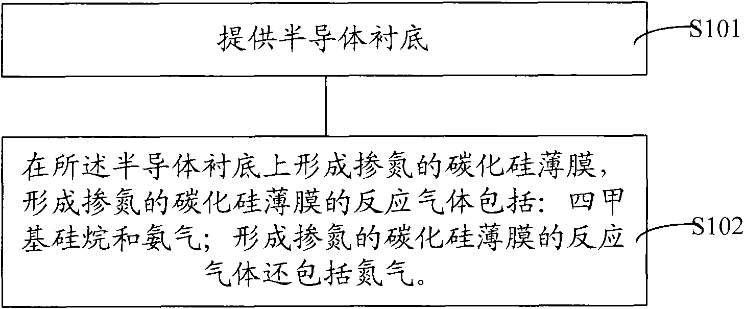
The invention relates to a forming method of a nitrogen-doped silicon carbide thin film, comprising the following steps of: providing a semiconductor substrate; and forming the nitrogen-doped silicon carbide thin film on the semiconductor substrate, wherein reaction gas used for forming the nitrogen-doped silicon carbide thin film comprises tetramethylsilane, ammonia gas and nitrogen gas. The nitrogen-doped silicon carbide thin film formed with the forming method of the invention has the advantages of small ranges of reflectivity difference values and good uniformity in properties.

Description

technical field [0001] The invention relates to the field of semiconductor manufacturing, in particular to a method for forming a nitrogen-doped silicon carbide film. Background technique [0002] In VLSI technology, silicon dioxide, which has thermal stability and moisture resistance, has always been the main dielectric material used between metal interconnection lines, and metal aluminum is the main material for circuit interconnection wires in chips. However, relative to the miniaturization of components and the increase in integration, the number of conductor connections in the circuit continues to increase, making the parasitic effects of resistance (R) and capacitance (C) in the conductor connection structure, causing serious problems. Transmission delay (RC Delay), in 130nm and more advanced technologies, becomes the main factor that limits the signal transmission speed in the circuit. [0003] Therefore, in terms of reducing wire resistance, metal copper has been wi...

Claims


Application Information

Patent Timeline
IPC IPC(8): H01L21/205H01L21/768
Inventor 周鸣
Owner SEMICON MFG INT (SHANGHAI) CORP
Why Eureka
Try Eureka