
Etching device of micro-nano ferroelectric domain structure based on atomic force microscope acoustic microscopy system

A technology of atomic force microscope and etching device, which is applied in the direction of microstructure device, manufacturing microstructure device, nanostructure manufacturing, etc., to achieve high-resolution imaging and evaluation, improve precision, and increase processing speed.

Active Publication Date: 2011-06-29
中科西卡思(苏州)科技发展有限公司
View PDF3 Cites 6 Cited by
  • Summary
  • Abstract
  • Description
  • Claims
  • Application Information

AI Technical Summary

Problems solved by technology

[0004] The invention uses a program-controllable high-pulse voltage application device to act on the conductive probe with a nanoscale radius of curvature, which solves the key technical problem of high-voltage application of microstructure processing that cannot be realized by the general AFM platform in the past; at the same time, the probe structure adopts The multi-probe structure realizes the high-efficiency and high-speed microfabrication of large-area nanostructures; in addition, the acoustic mode of the atomic force microscope can be used to realize high-resolution imaging of subsurface nanoferroelectric domain structures in situ to evaluate the structural integrity of microfabrication

Method used


Image

  • Etching device of micro-nano ferroelectric domain structure based on atomic force microscope acoustic microscopy system
  • Etching device of micro-nano ferroelectric domain structure based on atomic force microscope acoustic microscopy system
  • Etching device of micro-nano ferroelectric domain structure based on atomic force microscope acoustic microscopy system

Examples


Embodiment 1

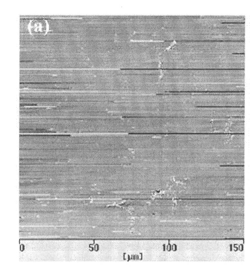
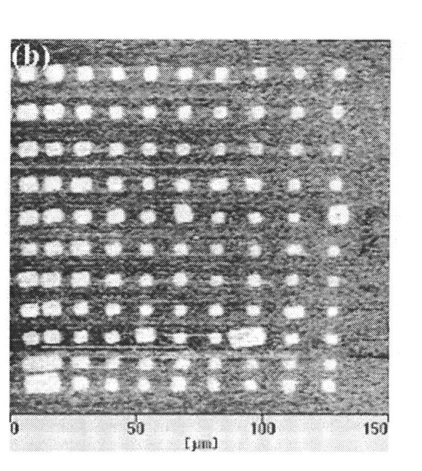
[0033]Embodiment 1: The microstructure processing of BMF ferroelectric single crystal is carried out by applying the nano-acoustic etching system constructed in the present invention, and Fig. 2 shows the test results. Figure 2(a) is the AFM image of the surface topography of the BMF single crystal sample, and Figure 2(b) is the acoustic imaging of the micromachined ferroelectric domain structure obtained in situ in the corresponding region of the sample. Obviously, Figure 2(a) is very different from Figure 2(b). The topography image 2(a) only shows the information of polishing scratches on the sample surface, while the acoustic image 2(b) clearly shows the dot-like ferroelectric domain array structure when the micromachining voltage is 190V / 10μs. Figure 2(c) is the acoustic image result of the column-like ferroelectric domain array microfabricated in another area of ​​the sample, and Figure 2(d) is the acoustic signal of the line A-B in Figure 2(c), showing that the column-li...

Embodiment 2

[0034] Embodiment 2: Application of the nanoacoustic etching system formed by the present invention to another BaTiO 3 Ferroelectric single crystal microstructure processing, Figure 3 shows the test results. Similar to Example 1 above, Fig. 3(a) is the AFM image of the surface topography of the sample, and Fig. 3(b) is the acoustic imaging of the micromachined ferroelectric domain structure obtained in situ in the corresponding region of the sample. Acoustic image Figure 3(b) clearly shows the ferroelectric domain array structure when the micromachining voltage is 230V / 5μs. The mechanism of the assembly of metal nanoparticles is also of great reference value.


PUM

PropertyMeasurementUnit
Elastic constantaaaaaaaaaa

Abstract

The invention relates to an etching device of a micro-nano ferroelectric domain structure based on an atomic force microscope acoustic microscopy system and belongs to the field of instrument development. The etching device comprises a microprocessing program control component, a pulse high-pressure excitation component, a multi-probe component and the atomic force microscope acoustic microscopy system. The etching device has the unique characteristics of nano-grade microprocessing, high pulse processing voltage, high-speed response, large-area microprocessing, high-resolution acoustic imaging of a microstructure and the like and is different from the microprocessing of the conventional commercial atomic force microscopes.

Description

technical field [0001] The invention relates to an etching device of a micro-nano ferroelectric domain structure based on an acoustic microsystem of an atomic force microscope, and belongs to the field of instrument development. Background technique [0002] Ferroelectrics random access memories (FRAM) are favored by major semiconductor companies in the United States, Japan, Europe and other countries because of their advantages such as non-volatility, low power consumption, radiation resistance, and high integration. As a non-volatile memory, FRAM is expected to become a new generation of memory products after flash memory (Flash) due to various performance advantages. The storage principle of FRAM is based on the physical characteristics of ferroelectric materials - the principle of polarization reversal of ferroelectric domains. The ferroelectric domain structure is the physical basis of the data storage unit (bit) of FRAM, and its polarization state will change with the...

Claims


Application Information

Patent Timeline
IPC IPC(8): B82B3/00B81C1/00B81C99/00
Inventor 曾华荣殷庆瑞刘黎明惠森兴李国荣
Owner 中科西卡思(苏州)科技发展有限公司
Learn More