Nanocrystalline silicon/crystalline silicon heterojunction photovoltaic cell
A photovoltaic cell and crystalline silicon technology, applied in the field of solar photovoltaic, can solve problems such as discontinuity of electric field, and achieve the effects of reducing interface recombination, good stability and low production cost
- Summary
- Abstract
- Description
- Claims
- Application Information
AI Technical Summary
Problems solved by technology
Method used
Image

Examples
Embodiment Construction
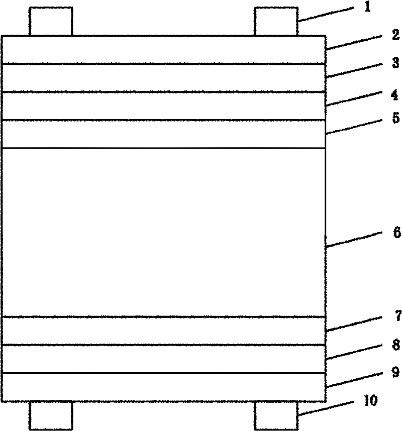
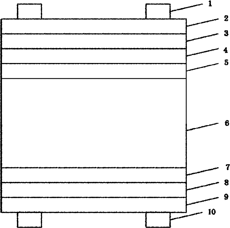
[0018] The stacking sequence of the present invention is as follows: front silver electrode, front TCO conductive film, p-type heavily doped nano-silicon layer, p-type lightly doped nano-silicon layer, p-type lightly diffused crystalline silicon layer, n-type crystalline silicon layer, this The structures of the nano-silicon layer, the n-type nano-silicon layer, the TCO conductive film on the back, and the silver electrode on the back are illustrated as examples. First, select n-type crystalline silicon wafers, perform the chemical cleaning process and texture in the production of conventional crystalline silicon cells, and then diffuse a low-concentration p-type layer on the n-type crystalline silicon wafers through the diffusion process, and then use RENA’s The wet etching process removes the back junction and edge pn junction, and then deposits a p-type lightly doped nano-silicon layer on the diffusion surface retained by the n-type crystalline silicon wafer using PECVD tech...
PUM
| Property | Measurement | Unit |
|---|---|---|
| Bandgap width | aaaaa | aaaaa |
| Thickness | aaaaa | aaaaa |
Abstract
Description
Claims
Application Information
 - R&D Engineer
- R&D Manager
- IP Professional
- Industry Leading Data Capabilities
- Powerful AI technology
- Patent DNA Extraction
Browse by: Latest US Patents, China's latest patents, Technical Efficacy Thesaurus, Application Domain, Technology Topic.
© 2024 PatSnap. All rights reserved.Legal|Privacy policy|Modern Slavery Act Transparency Statement|Sitemap