

Micro piezoresistive device for measuring wall shear stress and manufacturing method thereof
A measuring device and shear stress technology, applied in the field of sensors, can solve problems such as difficult process manufacturing, flow field interference, and low sensitivity, and achieve the effects of simple process, reduced bending stiffness, and high sensitivity
- Summary
- Abstract
- Description
- Claims
- Application Information
AI Technical Summary
Problems solved by technology
Method used
Image

Examples
Embodiment 1
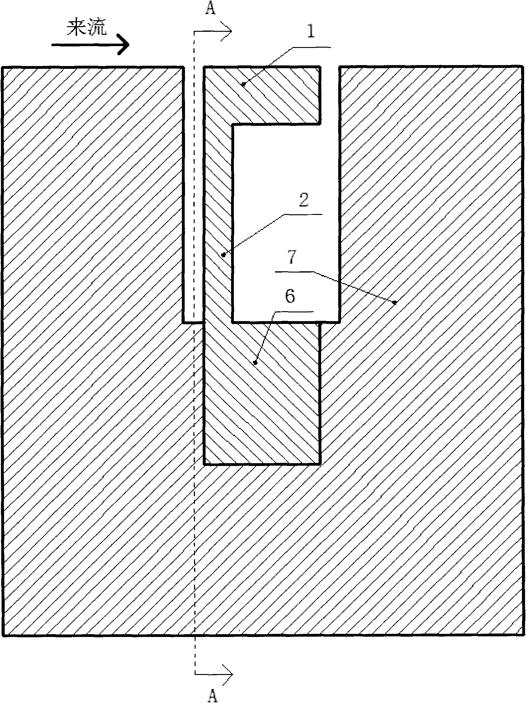
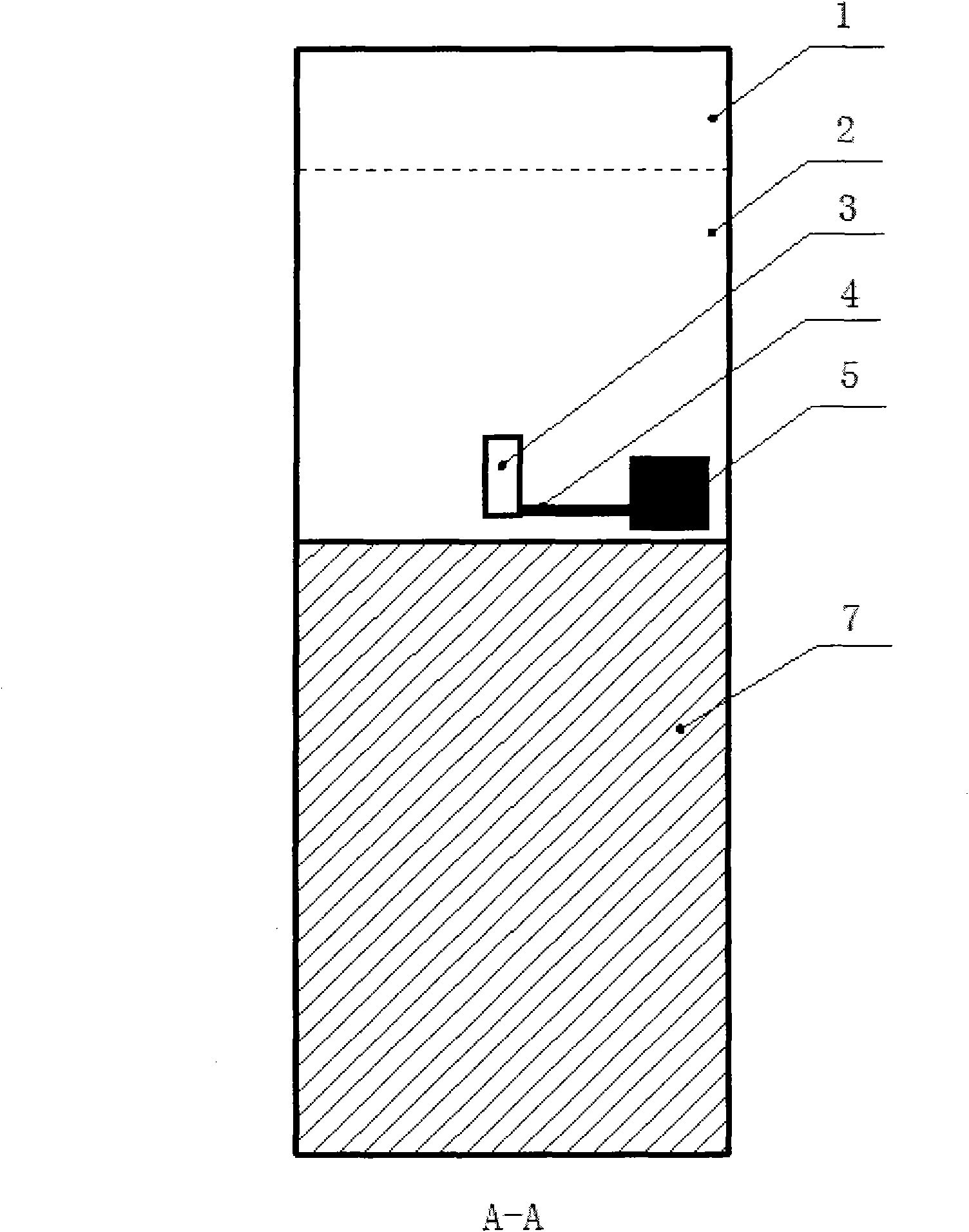
[0033] The measuring device in this embodiment is composed of a wall shear stress sensing part 1 , an elastic deformation part 2 , a piezoresistor 3 , wires 4 pads 5 , and a substrate 6 . A piezoresistor is made on the elastic deformation part 2, and is connected with an external measuring circuit through a wire 4 and a welding pad 5 to output an electric signal. The entire measuring device is pasted and fixed on a specific installation device through the base 6, and then the installation device is fixed at the position to be measured to realize measurement. After installation, the upper surface of the wall shear stress sensing part 1 is flush with the wall. The piezoresistor 3 is located at the bottom of the elastic deformation part. The material used in this device is silicon, which is processed by micro-processing technology. The main processing steps are as follows:
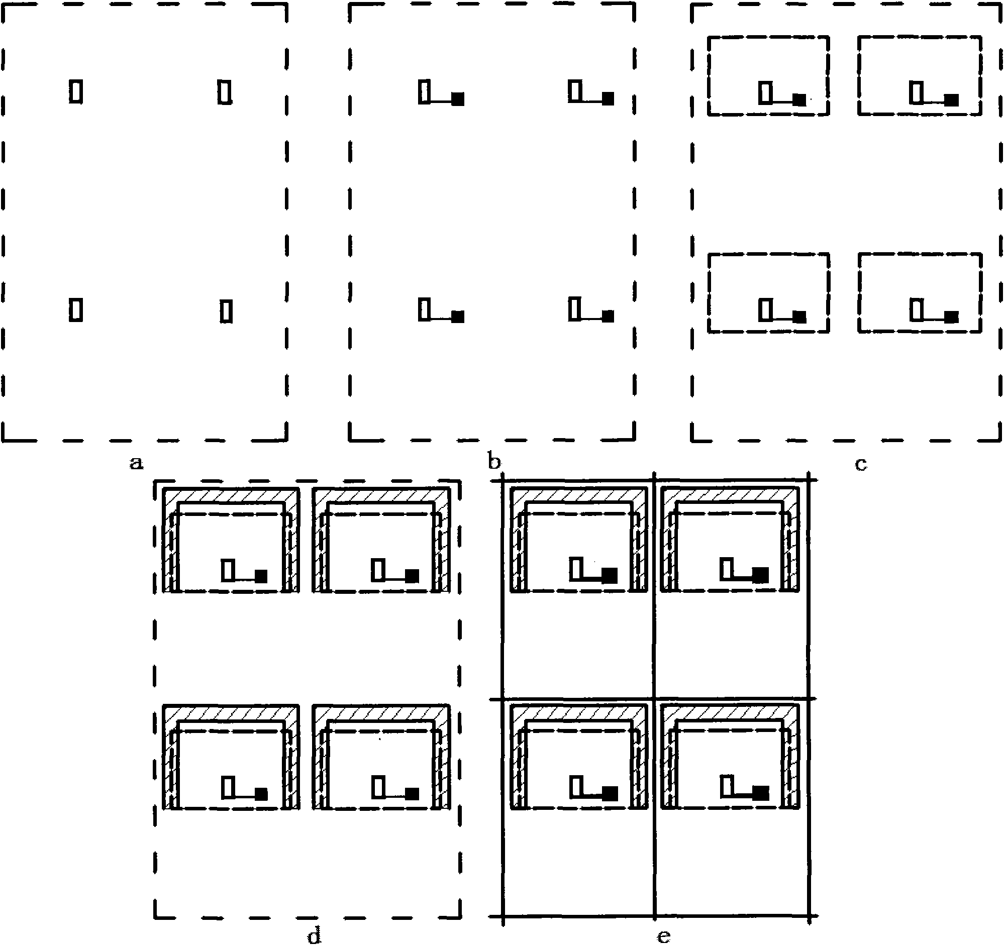
[0034] Step 1: Fabricate varistor 3 on the front side of the silicon wafer, see attached image 3 (a), ...
PUM
 Abstract
Description
Claims
Application Information