
High speed line parallel image sensor oriented to real-time vision chip

An image sensor and real-time vision technology, applied in the direction of image communication, color TV parts, TV system parts, etc., can solve the problems of insufficient speed, poor embedding, limiting system speed, etc., and achieve low cost and high integration , Improve the effect of sampled image quality

Active Publication Date: 2011-07-20
INST OF SEMICONDUCTORS - CHINESE ACAD OF SCI
View PDF5 Cites 21 Cited by
  • Summary
  • Abstract
  • Description
  • Claims
  • Application Information

AI Technical Summary

Problems solved by technology

There are several major problems in this way: 1) There is an I / O bottleneck between the large amount of image data sent by the camera and the computer, thereby limiting the speed of the system
Take the current mainstream USB2.0 interface as an example, its peak transmission speed is about 480Mbps, even if the megapixel image is compressed, its transmission speed is difficult to exceed 30 frames per second
2) Image processing requires a large number of repeated operations on all pixels. Even if these operations are completed by the current high-performance CPU, the speed is still not enough, and it is difficult to meet the real-time requirements
3) The power consumption of general-purpose computers is relatively large, and the embeddedness is poor

Method used


Image

  • High speed line parallel image sensor oriented to real-time vision chip
  • High speed line parallel image sensor oriented to real-time vision chip
  • High speed line parallel image sensor oriented to real-time vision chip

Examples


Embodiment Construction

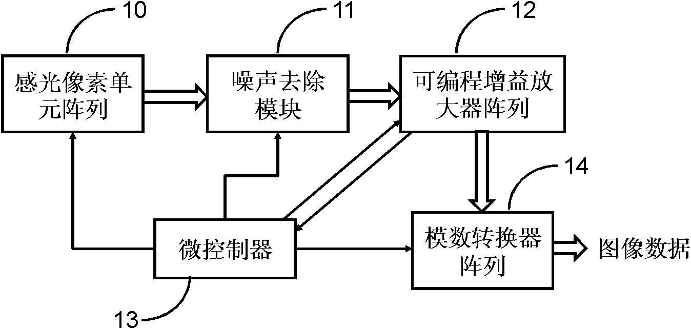
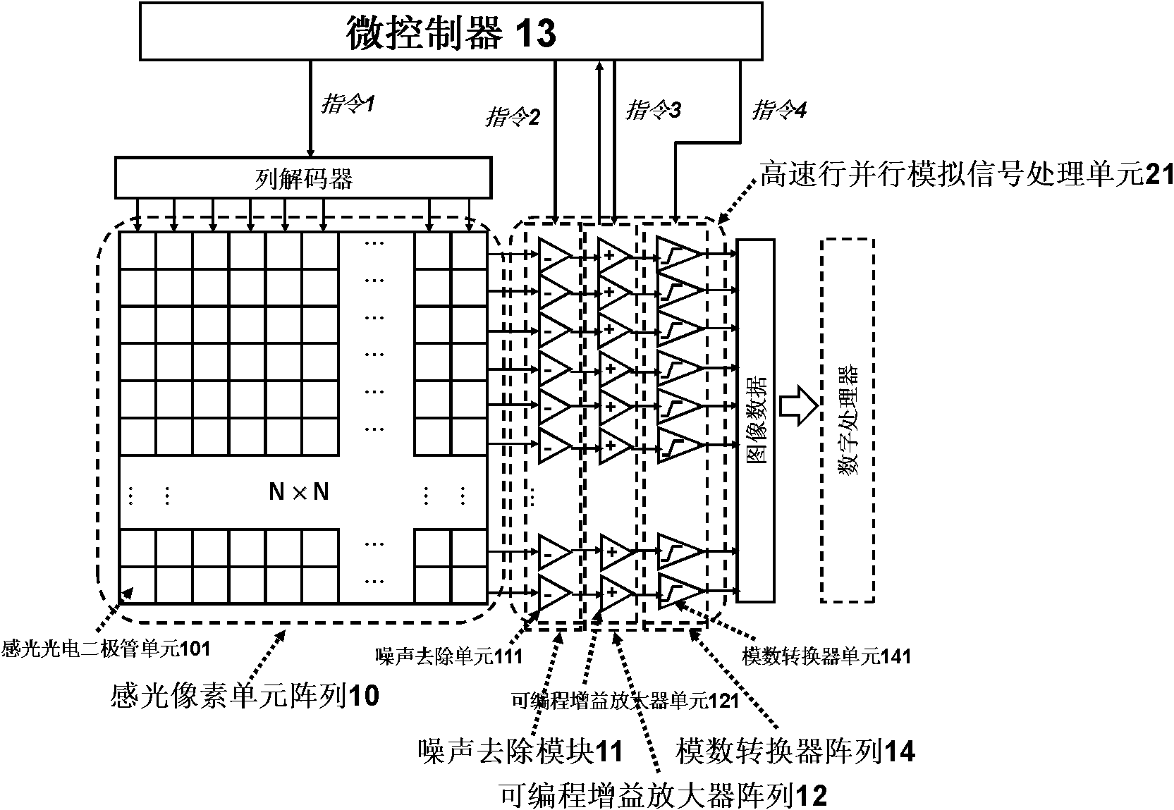
[0031] see figure 1 As shown, the present invention provides a kind of high-speed line parallel image sensor facing real-time vision chip, comprising:

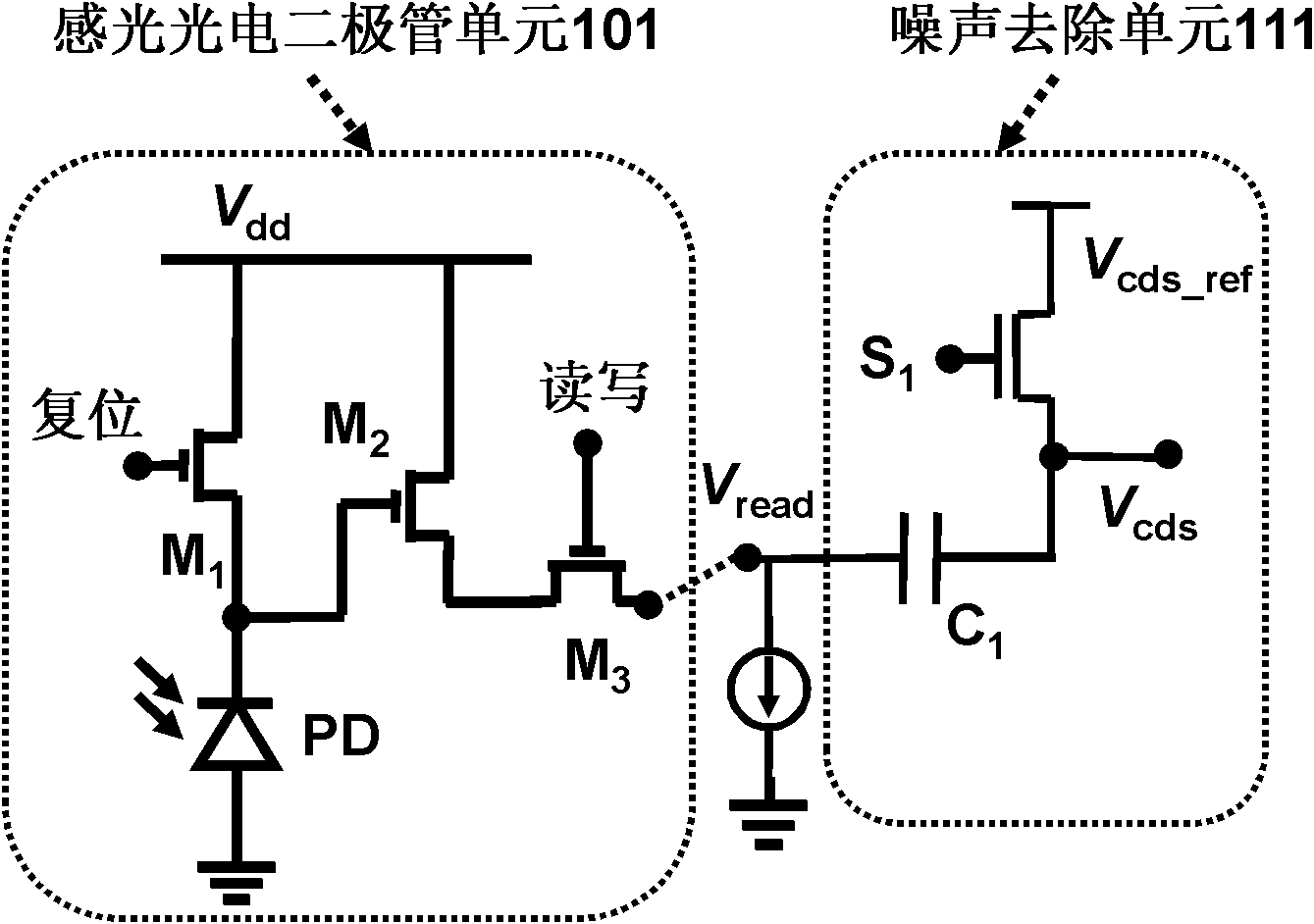
[0032] A photosensitive pixel unit array 10, used to collect the original information of the incident light, and convert the collected target image light signal into an electrical signal; the photosensitive pixel unit array 10 is composed of photosensitive photodiode units 101, each photosensitive photodiode The unit 101 is composed of a photosensitive photodiode part and a readout circuit part, and the photosensitive photodiode part is composed of a photodiode layer of a standard CMOS process, which is used to obtain higher light sensitivity at a lower cost; based on figure 1 The system block diagram of the high-speed line parallel image sensor facing the real-time vision chip, figure 2 The present invention provides a system structure diagram of a high-speed line-parallel image sensor oriented to a real-time vision chip, w...


PUM


Abstract

The invention discloses a high speed line parallel image sensor oriented to a real-time vision chip. The image sensor comprises a photosensitive pixel unit array, a noise removing module, a programmable gain amplifier array, an analog-to-digital converter array and a microcontroller, wherein the analog input end of the noise removing module is connected with the output end of the photosensitive pixel unit array; the analog input end of the programmable gain amplifier array is connected with the output end of the noise removing module; the analog input end of the analog-to-digital converter array is connected with the output end of the programmable gain amplifier array; the first output end of the microcontroller is connected with the input end of the photosensitive pixel unit array; the second output end of the microcontroller is connected with the digital input end of the noise removing module; the third output end of the microcontroller is connected with the digital input end of the programmable gain amplifier array; the fourth output end of the microcontroller is connected with the digital input end of the analog-to-digital converter array; and the input end of the microcontroller is connected with the feedback output end of the programmable gain amplifier array and is used for providing digital control commands for the photosensitive pixel unit array, the noise removing module, the programmable gain amplifier array and the analog-to-digital converter array and acquiring a feedback signal output by the programmable gain amplifier array.

Description

technical field [0001] The invention relates to the technical field of semiconductor CMOS image sensors, in particular to the technical field of high-speed real-time processing image sensors based on standard CMOS technology. Background technique [0002] The high-speed acquisition, processing and recognition of images by vision chips based on semiconductor CMOS image sensors has always been a problem of great significance. High-speed (>100 frames / second) image processing has many important applications in the fields of automobile control, industrial automation, and robot vision. The traditional vision system consists of a dedicated camera and a general-purpose computer, and uses software to complete image processing. There are several main problems in this way: 1) There is an I / O bottleneck between the large amount of image data sent by the camera and the computer, thereby limiting the speed of the system. Take the current mainstream USB2.0 interface as an example, its...

Claims


Application Information

Patent Timeline
IPC IPC(8): H04N5/374H04N5/357H04N5/3745
Inventor 付秋瑜吴南健林清宇张万成
Owner INST OF SEMICONDUCTORS - CHINESE ACAD OF SCI
Features
  • Generate Ideas
  • Intellectual Property
  • Life Sciences
  • Materials
  • Tech Scout
  • Unparalleled Data Quality
  • Higher Quality Content
  • 60% Fewer Hallucinations
Learn More