Seeding mold for growing silicon crystals by using orientated solidification method and crystal growing method

A mold and seeding technology, applied in the field of solar-grade silicon manufacturing equipment, to avoid spontaneous nucleation, eliminate dislocations, and be easy to process

Inactive Publication Date: 2012-12-19
GREENERGY CRYSTAL TECH
View PDF1 Cites 0 Cited by
  • Summary
  • Abstract
  • Description
  • Claims
  • Application Information

AI Technical Summary

Problems solved by technology

The seeding mold solves the problem of placing the seed crystal, and enables the seed crystal to eliminate dislocations during the seeding process, while avoiding the spontaneous nucleation of the melt on the bottom wall of the crucible. Therefore, this method does not need to change the existing directional solidification furnace and quartz The structure of the crucible can effectively grow monocrystalline silicon or quasi-monocrystalline silicon (that is, polycrystalline silicon ingots with large grains)

Method used


Image

  • Seeding mold for growing silicon crystals by using orientated solidification method and crystal growing method
  • Seeding mold for growing silicon crystals by using orientated solidification method and crystal growing method
  • Seeding mold for growing silicon crystals by using orientated solidification method and crystal growing method

Examples


Embodiment 1

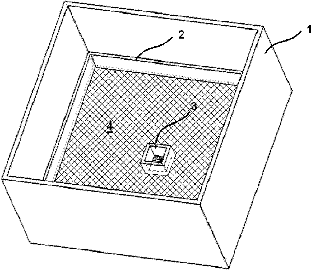
[0038] Such as image 3 and Figure 4 A kind of seeding mold 2 shown is processed by graphite material and placed in the bottom of prior art quartz crucible 1, including seed crystal container 3 and spacer liquid container 4, there is a square cylinder in the middle of seed crystal container 3 The first cavity is used to place the seed crystal 5, and the cross-sectional area of ​​the first cavity is 10000mm 2 , the height is 30mm, and the cross-sectional shape is a square; the spacer container 4 is formed by a cavity connected to the seed crystal container 3, and the cavity is surrounded by a graphite wall. Correspondingly, the bottom shape of the insulating liquid container 4 is adapted to the bottom shape of the quartz crucible 1 , so that the (liquid) insulating substance 8 placed in the insulating liquid container 4 can be separated from the bottom wall of the quartz crucible 1 . The upper part of the insulating liquid container 4 is open, and communicates with the inner...

Embodiment 2

[0045] Such as Figure 6 As shown, adopt the same method as that of Example 1, the difference is that in order to seed the crystal and better control the temperature gradient, the first cavity of the seed crystal container 3 has a section of diameter shrinkage near its top to form a long 10mm cavity. The necking section, the necking section itself is equal in diameter, but because the necking section has a gradually shrinking diameter, when the seed crystal grows through the narrow channel of the necking section, it can better eliminate the bit growth from the seed crystal. wrong.

[0046] In addition, a cavity is provided at the bottom of the seed crystal container 3, so that the temperature difference between the temperature at the position of the seed crystal 5 and the temperature around the quartz crucible 1 is larger, so that the temperature at the seed crystal 5 can be lowered when the silicon melt is kept overheated. Right around the melting point.

[0047] A further ...

example example 3

[0049] In the same manner as in Example 1, the difference is that the spacer 8 used is 6N high-purity germanium (Ge, with a purity of 99.9999%) and 5N high-purity lead (Pb, with a purity of 99.999%). The mass percentage is 1: 1 mixture.


PUM

PropertyMeasurementUnit
areaaaaaaaaaaa
heightaaaaaaaaaa
thicknessaaaaaaaaaa

Abstract

The invention discloses a seeding mold for growing silicon crystals by using an orientated solidification method and a crystal growing method. The seeding mold is arranged at the internal bottom of a quartz crucible and comprises a seed crystal container and a sealing liquid container, wherein the sealing liquid container consists of cavities connected to the periphery of the seed crystal container and is used for accommodating a sealing substance; and the seed crystal container is provided with a first cavity for accommodating seed crystals. A method for growing monocrystalline silicon / similar monocrystalline silicon by adopting the seeding mold comprises the following steps of: arranging or setting the seeding mold at the bottom of the quartz crucible; arranging the sealing substance and the seed crystals in the sealing liquid container and the seed crystal container respectively; putting a silicon raw material into the quartz crucible; and growing monocrystals / similar monocrystals by adopting orientated solidification. By adopting the seeding mold and the crystal growing method, the problem of placement of the seed crystals can be solved without changing the structures of the conventional orientated solidification and quartz crucible, dislocation of the seed crystals in the seeding process is eliminated, and the spontaneous nucleation phenomenon of melt from the bottom wallface of the crucible is avoided. The seeding mold has low cost and is easy to process.

Description

technical field [0001] The invention belongs to the field of solar-grade silicon manufacturing equipment and methods, and in particular relates to a seeding mold for growing silicon crystals by directional solidification, and a method for growing single crystal silicon / single crystal silicon using the seeding mold. Background technique [0002] Silicon single crystal and silicon polycrystalline ingot are the most commonly used materials for crystalline silicon solar cells. Generally, solar cells manufactured using silicon single crystal materials have higher photoelectric conversion efficiency than solar cells manufactured using silicon polycrystalline materials. At present, the most commonly used manufacturing methods for silicon single crystal are pulling method (Czochralski method) and zone melting method (Floating Zone method); the manufacturing method for silicon polycrystal usually adopts directional solidification method (ie casting method). The directional solidific...

Claims


Application Information

Patent Timeline
Patent Type & Authority Patents(China)
IPC IPC(8): C30B11/00C30B29/06
Inventor 李乔马远
Owner GREENERGY CRYSTAL TECH
Why Eureka
Try Eureka