
Grid enhanced-power semiconductor field effect transistor

A technology of field effect transistors and power semiconductors, which is applied in semiconductor devices, electrical components, circuits, etc., can solve the problems of large area occupied by side oxygen structures, improve the area occupied by large areas, increase the concentration of drift regions, and reduce the conductivity. The effect of on-resistance

Inactive Publication Date: 2013-03-06
HARBIN ENG UNIV
View PDF1 Cites 4 Cited by
  • Summary
  • Abstract
  • Description
  • Claims
  • Application Information

AI Technical Summary

Problems solved by technology

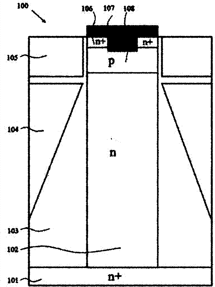
[0005] However, both GOB and SGE use the side oxygen structure. On the one hand, there is a certain process difficulty in the formation of oblique side oxygen; on the other hand, the side oxygen structure occupies a large area.

Method used


Image

  • Grid enhanced-power semiconductor field effect transistor
  • Grid enhanced-power semiconductor field effect transistor
  • Grid enhanced-power semiconductor field effect transistor

Examples


Embodiment 1

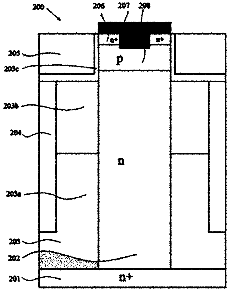
[0026] refer to image 3 . image 3 In the above, the dielectric layer 203 is divided into three sections 203a, 203b, and 203c. The gate dielectric part is also counted as a section. The thickness of the dielectric layer 203 is 0.5 μm, and the K value of each section of the medium is different. The K value of the 203a section is 2.2, and the section length is 3.5 μm; the K value of the 203b section is 5.06, and the section length is 1.5 μm; the K value of the 203c section twenty one. The width of the drift region 202 is the same as figure 1 is 0.8 μm, and its doping concentration is 4.0×10 16 cm -3 . Breakdown voltage is the same as figure 1 Under the structure of 119V, the corresponding FOM=63.8MW / cm 2 .

Embodiment 2

[0028] refer to Figure 4 . Figure 4 , the dielectric layer 203 is divided into 4 sections, 203-1, 203-2, 203-3, and 203-4, and the gate dielectric part is also counted as a section. image 3 an extra paragraph. Except for the K value distribution of the dielectric layer (203) and the doping concentration of the drift region 202, other parameters and image 3 in the same. K value distribution: the K value of the 203-1 segment is 2.9, and the segment length is 2.75 μm; the K value of the 203-2 segment is 5.8, and the segment length is 1.25 μm; the K value of the 203-3 segment is 11.6, and the segment length is 1.0 μm; the K value of segment 203-4 was 23.2. The doping concentration of the drift region (202) is 6.0×10 16 cm -3 . When the breakdown voltage is the same as 119V, the corresponding FOM=84.8MW / cm 2 .


PUM


Abstract

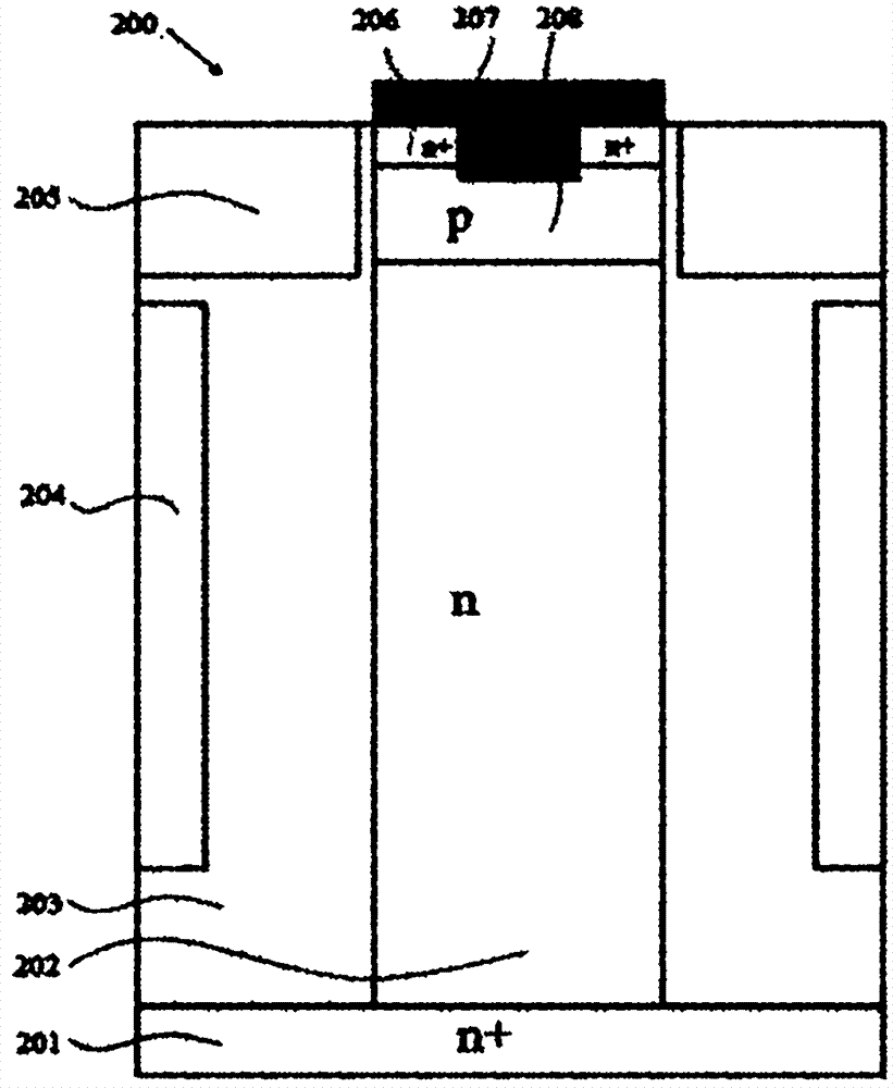
The invention provides a grid enhanced-power semiconductor field effect transistor which comprises a drain region (201), a drift region (202), a dielectric layer (203), a split grid (204), a grid electrode (205), an n+ layer (206), a source electrode (207) and a channel region (208), wherein K values of the dielectric layer (203) are distributed according to a certain law, namely, the K values become smaller from the source electrode to the drain electrode. In the grid enhanced-power semiconductor field effect transistor, the dielectric layer, the K values of which are distributed according to a certain law, is used for replacing an original side oxide structure, therefore, the drain-source on resistance is reduced on the condition that the withstand voltage of a device is not sacrificed. The transistor is compatible with the conventional MOSFET (metal-oxide-semiconductor field effect transistor) process, has very strong feasibility and can meet the application requirements of a power electronic system more easily.

Description

technical field [0001] The present invention relates to a vertical metal oxide semiconductor field effect transistor (Vertical MOSFET), in particular to an improved gate-enhanced power MOSFET. Background technique [0002] In the field of power electronics, power MOSFETs are widely used in switching device structures. In order to make the switching device function well, the power MOSFET needs to meet two requirements: 1. When the device is in the on state, it can have a very low on-resistance to minimize the power loss of the device itself; 2. When the device is in the on state In the off state, it can have a high enough reverse breakdown voltage. Yung C. Liang proposed a new device to replace Super Junction in the low-voltage range, called Gradient 0xide-Bypassed (abbreviated as GOB) structure device (Yu Chen, Yung C. Liang and G.S. Samudra: IEEE Transactions on Power Electronics 22(4)2007). The GOB structure translates the impurity concentration matching problem, which ...

Claims


Application Information

Patent Timeline
Patent Type & Authority Patents(China)
IPC IPC(8): H01L29/78H01L29/51H01L29/06H01L29/423
Inventor 王颖兰昊曹菲刘云涛邵雷
Owner HARBIN ENG UNIV
Learn More