Amorphous silicon image sensor with storage capacitor structure

An image sensor and storage capacitor technology, applied in radiation control devices and other directions, can solve the problems of reducing the capacitance of photodiodes, reducing the effective area of ​​photodiodes, and reducing the ability of photodiodes to store charges, so as to improve the dynamic range of signals and increase the charge storage capacity. Effect

Active Publication Date: 2013-07-17
CARERAY DIGITAL MEDICAL TECH CO LTD
View PDF5 Cites 0 Cited by
  • Summary
  • Abstract
  • Description
  • Claims
  • Application Information

AI Technical Summary

Problems solved by technology

[0004]With the continuous improvement of semiconductor manufacturing technology and the continuous improvement of image resolution requirements, the size of the pixel unit of the amorphous silicon image sensor is gradually reduced, but the reduction The size of the pixel unit will inevitably reduce the effective area of ​​the photodiode, thereby reducing the capacitance on the photodiode, and the reduction of the capacitance will reduce the charge storage capacity between the upper and lower electrodes of the photodiode, and finally lead to the output signal of the amorphous silicon image sensor. drop in dynamic range

Method used


Image

  • Amorphous silicon image sensor with storage capacitor structure
  • Amorphous silicon image sensor with storage capacitor structure
  • Amorphous silicon image sensor with storage capacitor structure

Examples


Embodiment 1

[0061] The specific process steps in the first embodiment are as follows:

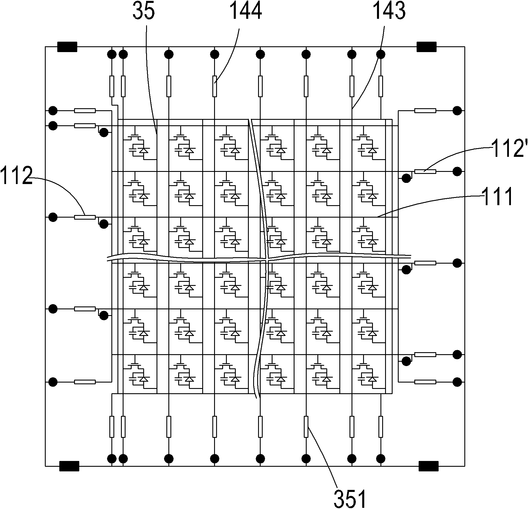
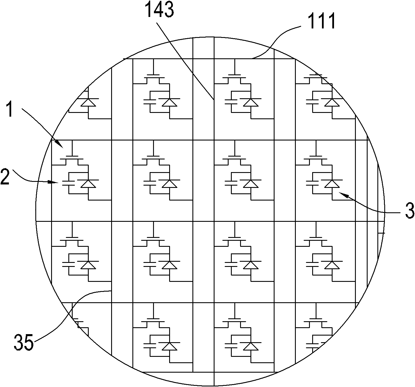
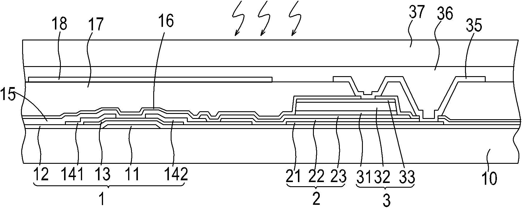
[0062] (1) As attached Image 6 And Figure 16 As shown, a first layer of metal is deposited on a glass substrate 10, and an etching process is used to form a gate electrode 11 and a gate line 111;

[0063] (2) As attached Figure 7 , 8 As shown in Figure 17, a first insulating layer 12 is formed on a glass substrate 10, an active layer 13 composed of an intrinsic amorphous silicon film and an n-type amorphous silicon film is formed, and the active layer 13 is etched to form a silicon island using a photolithography process ;

[0064] (3) Deposit the second layer of metal;

[0065] (4) As attached Picture 9 , 18 As shown, the data line 143, the drain electrode 141, the source electrode 142, and the lower electrode 21 of the storage capacitor are formed by an etching process. At this time, the thin film transistor 1 has been formed;

[0066] (5) Depositing the second insulating layer 15,

[0067] (6) See a...


PUM


Abstract

The invention relates to an amorphous silicon image sensor with a storage capacitor structure, comprising a plurality of pixel units. Each pixel unit comprises a grid wiring, a first insulating layer, an active layer, a data wiring, a second insulating layer, a storage capacitor, a photosensitive diode, a passivation layer and a bias voltage wire, wherein the storage capacitor is arranged below the photosensitive diode; a lower electrode of the storage capacitor is formed on a glass substrate or the first insulating layer, and an upper electrode of the storage capacitor is formed on a dielectric layer and connected with a source electrode; a first electrode of the photosensitive diode is in co-electrode with the upper electrode of the storage capacitor; and a second electrode of the photosensitive diode is conductive with the lower electrode of the storage capacitor and the bias voltage wire. By means of the amorphous silicon image sensor disclosed by the invention, the charge storagecapacity of the pixel units is increased under the condition of not enlarging or reducing pixel dimensions by arranging the storage capacitor below the photosensitive diode, and therefore the purposeof enhancing the signal dynamic range of a thin film transistor matrix panel under the precondition of not losing the resolution ratio of the thin film transistor matrix panel is achieved.

Description

technical field [0001] The invention relates to a semiconductor device, in particular to an amorphous silicon image sensor with a storage capacitance structure applied to an X-ray detector. Background technique [0002] Image sensors are mainly used to collect light signals and convert them into electrical signals, and read out the above electrical signals through integrated circuits to obtain the collected images. [0003] For example, the Chinese patent application number 200380106054.6 discloses an X-ray detector, which includes a thin-film transistor array panel (amorphous silicon image sensor), an X-ray generator, a reading circuit, and a gate driver. The thin-film transistor array panel It includes a plurality of pixel units for detecting X-rays generated by the X-ray generator, and each pixel unit includes a photosensitive diode (PD) and a thin-film transistor (TFT), which is used to convert the electrical signal output from the photodiode . The read circuit is used...

Claims


Application Information

Patent Timeline
Patent Type & Authority Patents(China)
IPC IPC(8): H01L27/146
Inventor 刘建强王恒和
Owner CARERAY DIGITAL MEDICAL TECH CO LTD
Why Eureka
Try Eureka