Method for manufacturing bottom gate metal oxide thin film transistor

A technology of oxide thin films and transistors, applied in the direction of transistors, semiconductor/solid-state device manufacturing, semiconductor devices, etc., to reduce stress concentration, improve production pass rate, and solve the effects of easy fracture

Active Publication Date: 2013-07-10
广东芯聚能半导体有限公司
View PDF4 Cites 0 Cited by
  • Summary
  • Abstract
  • Description
  • Claims
  • Application Information

AI Technical Summary

Problems solved by technology

When the device is used for flat panel display driving, the above cracks can lead to the occurrence of point defects

Method used


Image

  • Method for manufacturing bottom gate metal oxide thin film transistor
  • Method for manufacturing bottom gate metal oxide thin film transistor
  • Method for manufacturing bottom gate metal oxide thin film transistor

Examples


Embodiment 1

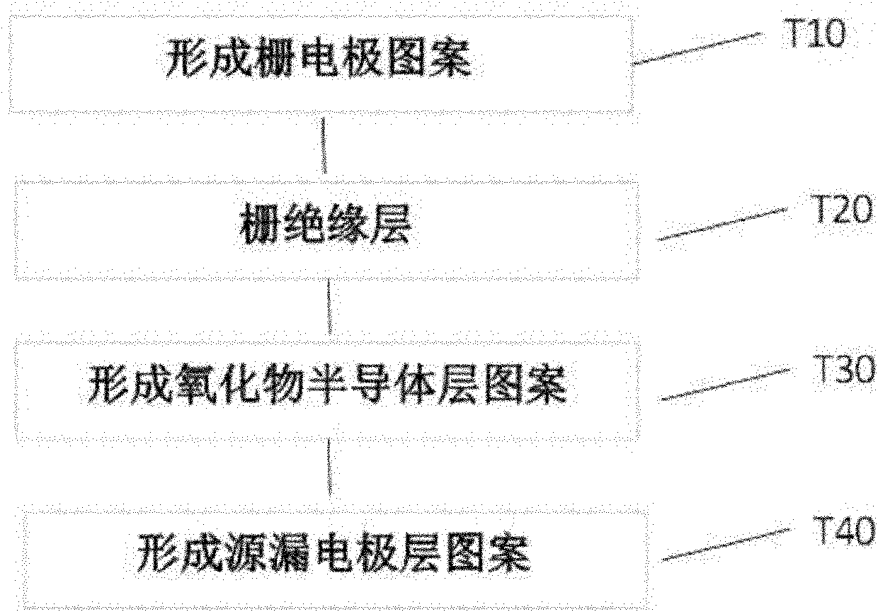
[0030] Such as Figure 4 As shown, the manufacturing process of the bottom gate metal oxide thin film transistor of the present invention comprises the following steps:

[0031] a) Deposit a layer of gate electrode film on the glass substrate and form the desired pattern through processes such as photolithography and etching (such as Figure 4 (a) shown).

[0032] b) Deposit a layer of gate insulating layer material (such as Figure 4 (b) shown).

[0033] c) Deposit a layer of metal oxide material to make it an insulator by controlling the process conditions (such as Figure 4 (c) shown).

[0034] d) Apply photoresist 710 and use chemical mechanical polishing (CMP) technology to planarize the photoresist, so that other areas except the vicinity of the channel area are covered by photoresist (as shown in 4(d)) .

[0035] e) Treating the exposed oxide film to transform it into a semiconductor characteristic by adopting vacuum annealing method 810 (as shown in 4(e)).

[00...

Embodiment 2

[0046] Such as Figure 5 As shown, the process flow of this embodiment is similar to that of embodiment 1. The difference is in Figure 5 In (e), the method (820) of annealing treatment in a reducing atmosphere is adopted to realize the transformation of the metal oxide from an insulator to a semiconductor.

[0047] In the process step 820, the sample is heated to 300° C. under a reducing atmosphere such as hydrogen or nitrogen, kept for 30 minutes, and then cooled in air. Increase the carrier concentration of the treated metal oxide film to 10 13 ~10 15 cm -3 In the range, it exhibits semiconducting properties.

Embodiment 3

[0049] Such as Figure 6 As shown, the process flow of this embodiment is similar to that of Embodiment 1. The difference is in Figure 6 In (e), the plasma treatment method (830) is used to realize the transformation of the metal oxide from an insulator to a semiconductor.

[0050] In the process step 830, the sample is placed in a vacuum chamber, and the surface of the sample is treated with argon plasma for 3-5 minutes, and the discharge power is 150W. Increase the carrier concentration of the treated metal oxide film to 10 13 ~10 15 cm -3 In the range, it exhibits semiconducting properties.

[0051] By adopting the process flow in the above-mentioned embodiments 1-3, the process steps of photolithography and etching of the active layer are saved, and chemical mechanical polishing and annealing (or plasma treatment) processes are used instead, which is more efficient. figure 2 The traditional process shown is simple.

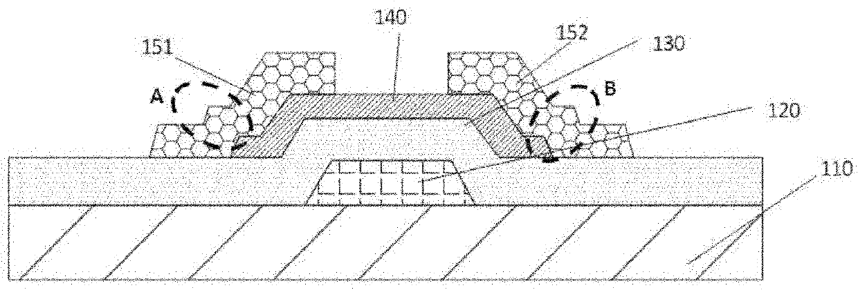
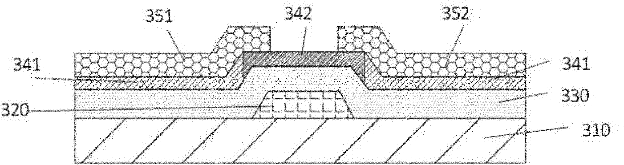
[0052] image 3 It is a schematic structural d...


PUM

PropertyMeasurementUnit
thicknessaaaaaaaaaa
thicknessaaaaaaaaaa
thicknessaaaaaaaaaa

Abstract

The invention relates to a method for manufacturing a bottom gate metal oxide thin film transistor in the technical field of semiconductor manufacturing. The method comprises the following steps: sequentially manufacturing a gate electrode and a metal oxide material; then coating an optical resist on the surface of the metal oxide material and the optical resist, and carrying out planarization treatment on the optical resist by adopting chemical machinery polishing; carrying out annealing treatment or plasma treatment on the metal oxide which is not masked by the optical resist; and finally stripping the optical resist, then carrying out magnetron sputtering and deposition on the source electrode and the drain electrode materials, and forming the source electrode and the drain electrode through photoetching and wet process etching. According to the invention, the characteristic that the metal oxide material can be converted from an insulator into a semiconductor after special treatment is utilized, the metal oxide thin film transistor with an active layer of a special structure is manufactured, and the occurrence of the crack phenomenon of the source electrode and the drain electrode can be prevented effectively.

Description

technical field [0001] The invention relates to a method for preparing a transistor in the field of semiconductor technology, in particular to a method for preparing a bottom-gate metal oxide thin film transistor. Background technique [0002] At present, semiconductor materials such as amorphous silicon (a-Si) and polycrystalline silicon (p-Si) are mostly used in the active layer of the thin film transistor (TFT) technology. Among them, a-Si TFT is the most widely used and can cover almost all sizes of flat panel display (FPD) products. Limited by the uniformity of film quality, p-Si TFT is currently only suitable for small and medium-sized products. In terms of device characteristics, a-Si TFT has the advantages of simple structure and good mass production uniformity, but it also has low mobility (about 0.5cm 2 / V·s), poor light stability and other disadvantages; although p-Si TFT has much higher mobility than a-Si TFT (>10cm 2 / V·s), but at the same time has the dis...

Claims


Application Information

Patent Timeline
Patent Type & Authority Patents(China)
IPC IPC(8): H01L29/786H01L29/06H01L21/34
Inventor 董承远施俊斐
Owner 广东芯聚能半导体有限公司
Why Eureka
Try Eureka