Method and device for manufacturing field-effect transistor
A field-effect transistor and manufacturing method technology, applied in transistors, semiconductor/solid-state device manufacturing, semiconductor devices, etc., can solve problems such as long time, decreased production efficiency, and loss of quality of active layer thin films.
- Summary
- Abstract
- Description
- Claims
- Application Information
AI Technical Summary
Problems solved by technology
Method used
Image

Examples
no. 1 approach
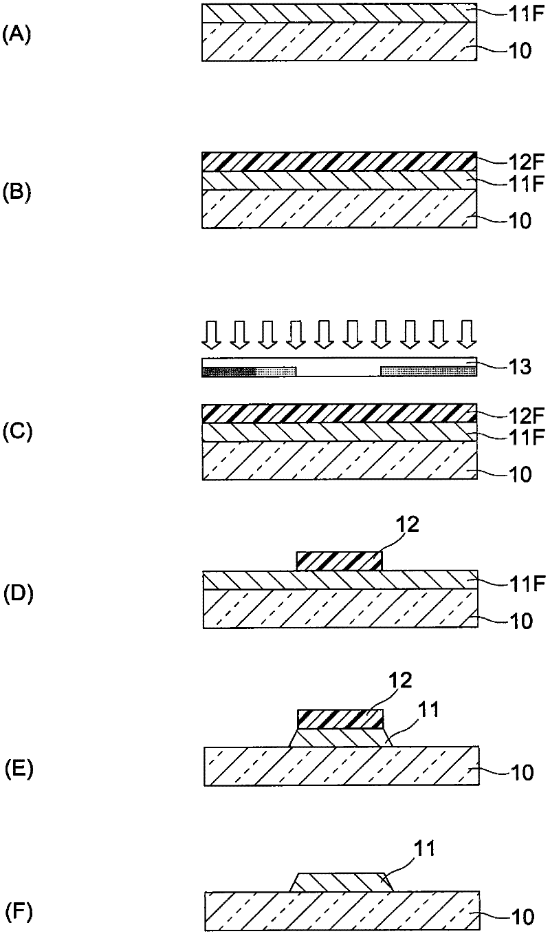
[0061] Figure 1 to Figure 5 It is a sectional view showing main parts for explaining each process of the method of manufacturing the field effect transistor according to the first embodiment of the present invention. In this embodiment mode, a method of manufacturing a field effect transistor having a so-called bottom-gate transistor structure will be described.
[0062] Such as figure 1 As shown in (A), first, the gate electrode film 11F is formed on one surface of the substrate 10 .
[0063] A typical substrate 10 is a glass substrate. A typical gate electrode film 11F is composed of a metal single-layer film or a metal multi-layer film of molybdenum, chromium, aluminum, etc., and is formed by, for example, sputtering. The thickness of the gate electrode film 11F is not particularly limited, and it is, for example, 300 nm.
[0064] Next as figure 1 Medium (B)~ figure 1 As shown in (D), the gate electrode film 11F is processed into a resist mask 12 for patterning havin...
no. 2 approach
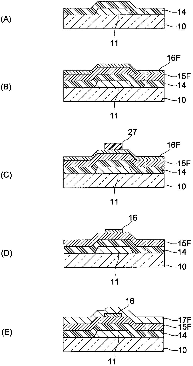
[0103] Figure 7 The second embodiment of the present invention is shown. In addition, in the drawings, parts corresponding to the above-mentioned first embodiment are denoted by the same reference numerals, and detailed description thereof will be omitted.
[0104] The transistor element 101 in this embodiment is produced through the same steps as those in the first embodiment. The difference between the illustrated transistor element 101 and the transistor element 100 in the first embodiment described above is that the barrier layer 16 has a multilayer structure composed of a first insulating film 16A and a second insulating film 16B.
[0105] The semiconductor layer containing zinc (Zn) has weak acid and alkali resistance, so it is easy to be etched. Therefore, a barrier layer 16 is formed in the trench region of the IGZO film 15F to prevent corrosion by an etchant when forming the active layer 15 . The barrier layer 16 functions as both an etching mask for the IGZO film...
no. 3 approach
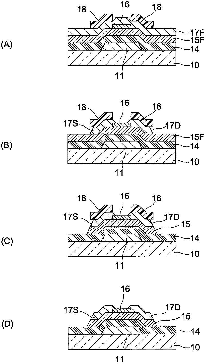
[0116] Figure 9 The third embodiment of the present invention is shown. In addition, in the drawings, parts corresponding to the above-mentioned first and second embodiments are assigned the same reference numerals, and detailed description thereof will be omitted.
[0117] The transistor element 102 in this embodiment is produced through the same steps as those in the first embodiment. The difference between the illustrated transistor element 102 and the transistor element 101 in the above-described second embodiment is that the gate insulating film 14 has a multilayer structure composed of a first gate insulating film 14A and a second gate insulating film 14B.
[0118] The purpose of forming the gate insulating film is to ensure an electrically insulating state between the gate electrode and the active layer. However, since the gate insulating film made of a silicon oxide film has a low barrier to the diffusion of impurities from the substrate (substrate), when impurities...
PUM
 Abstract
Description
Claims
Application Information
 - R&D
- Intellectual Property
- Life Sciences
- Materials
- Tech Scout
- Unparalleled Data Quality
- Higher Quality Content
- 60% Fewer Hallucinations
Browse by: Latest US Patents, China's latest patents, Technical Efficacy Thesaurus, Application Domain, Technology Topic, Popular Technical Reports.
© 2025 PatSnap. All rights reserved.Legal|Privacy policy|Modern Slavery Act Transparency Statement|Sitemap|About US| Contact US: help@patsnap.com