Film transistor substrate and display device thereof

A technology for thin film transistors and substrates, applied in transistors, electro-solid devices, semiconductor devices, etc., can solve the problems of hindering metal layers, reducing productivity, increasing manufacturing costs, etc., and achieving the effects of low contact resistivity, high adhesion and

Inactive Publication Date: 2011-08-31
KOBE STEEL LTD
View PDF11 Cites 6 Cited by
  • Summary
  • Abstract
  • Description
  • Claims
  • Application Information

AI Technical Summary

Problems solved by technology

[0005] First, when the Cu-based alloy wiring film is brought into direct contact with the semiconductor layer of the TFT without interfering with the barrier metal layer, the subsequent process (for example, the film formation process of the insulating film formed on the TFT or the heat of sintering or annealing) process), Cu in the Cu-based alloy wiring film diffuses in the semiconductor layer, TFT characteristics decrease, or the contact resistance between the Cu-based alloy wiring film and the semiconductor layer increases
[0006] Second, as described above, when Cu in the Cu-based alloy wiring film diffuses in the semiconductor to form a reaction layer between the semiconductor layer and Cu, there is a problem that the Cu-based alloy wiring film is partially peeled off from the reaction layer.
Specifically, it is necessary to use a film forming apparatus (a representative cluster tool in which a plurality of film forming chambers are connected to a transfer chamber) equipped with a film forming chamber for hindering the formation of the metal layer must be used, resulting in a decrease in manufacturing cost. up and down in productivity

Method used


Image

  • Film transistor substrate and display device thereof
  • Film transistor substrate and display device thereof
  • Film transistor substrate and display device thereof

Examples


Embodiment 1

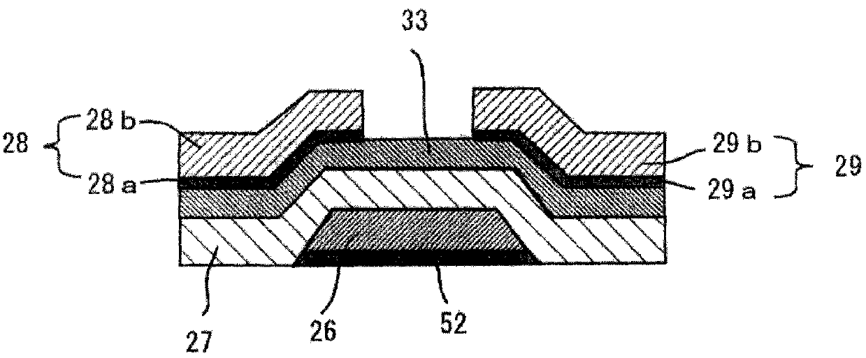
[0092] In this example, the contact resistivity and adhesion between the Cu alloy layer (laminated structure) and the semiconductor layer will be discussed.

[0093] (1) Measurement of contact resistivity with semiconductor layer

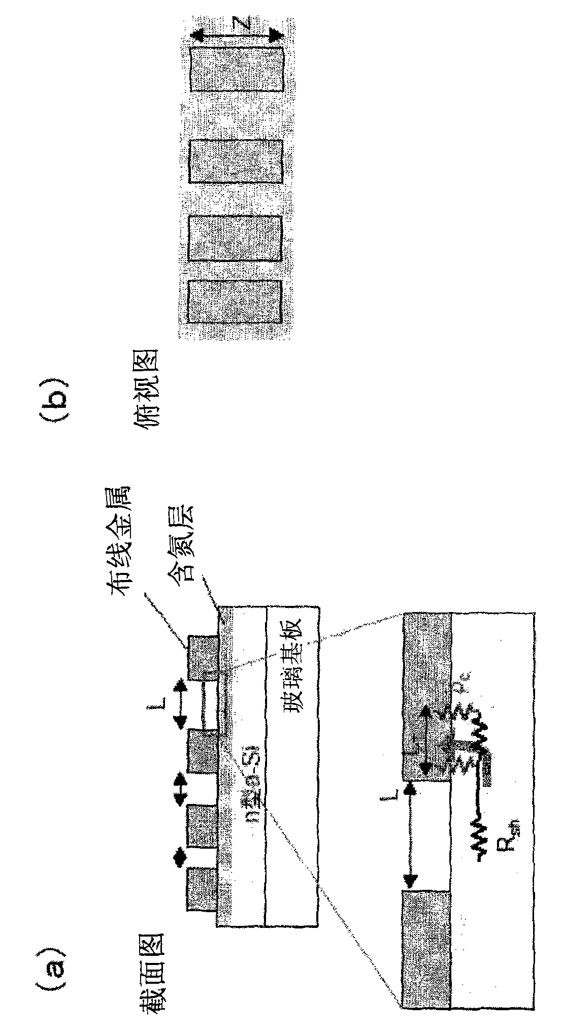
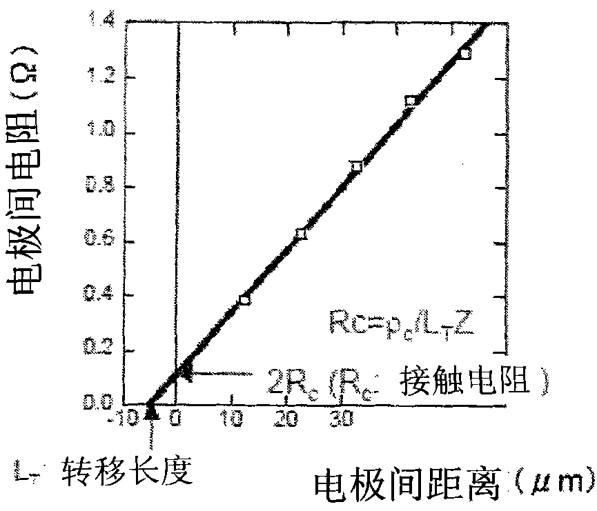
[0094] In order to investigate the contact resistivity between the Cu alloy layer and the semiconductor layer, a TLM (TransferLengthMethod) element was produced, according to figure 2 , 3 The TLM method is shown for the determination of contact resistivity. First, a method of fabricating a TLM element will be described.

[0095] First, a low-resistance amorphous silicon film doped with an impurity (P) with a thickness of about 200 nm is formed on a glass substrate by plasma CVD to a thickness of about 200 nm. Next, in the same plasma CVD apparatus, only oxygen was supplied to generate plasma, and the surface of the low-resistance amorphous silicon film was treated with oxygen plasma for 30 seconds to form an oxygen-containing layer. As an oxyge...

Embodiment 2

[0123] In this example, the oxygen-containing layer formed on the surface of the semiconductor layer prevents Cu atoms in the Cu alloy layer from diffusing into the semiconductor layer.

[0124] First, a SiN film with a film thickness of approximately 100 nm is formed on a glass substrate by plasma CVD, and a low-resistance amorphous silicon film (n-a-Si:H layer) doped with impurities (P) with a film thickness of 200 nm is formed thereon. . The film formation temperature of plasma CVD was 320°C.

[0125] Next, only oxygen was supplied into the same chamber of the same plasma CVD apparatus to generate plasma, and the surface of the aforementioned low-resistance amorphous silicon film was treated with oxygen plasma for 10 minutes to form an oxygen-containing layer. As the oxygen plasma device, a measuring device (model: PR41) manufactured by Yamato Science Co., Ltd. was used. The frequency was 13.56 Hz, the input power was 450 W, the film formation temperature was room temperat...

Embodiment 3

[0133] In this example, the influence of the [O] / [Si] ratio in the oxygen-containing layer and the film thickness of the oxygen-containing layer on the contact resistivity and adhesion will be discussed.

[0134] (1) Measurement of the bonding state of O and Si in the oxygen-containing layer

[0135] The preparation of the sample was the same as the adhesion evaluation test of Example 1, except that the Cu alloy layer was used as the first layer: Cu-4atom% Mn (film thickness: 20nm), and the second layer: pure Cu (film thickness: 280nm). . In addition, the oxygen flow rate in the oxygen plasma treatment was 30 sccm.


PUM

PropertyMeasurementUnit
thicknessaaaaaaaaaa
thicknessaaaaaaaaaa
thicknessaaaaaaaaaa

Abstract

The invention provides a film transistor substrate which has a low contact resistivity and good space continuity even a Cu series alloy wiring film directly contacts with a semiconductor. The film transistor substrate comprises a semiconductor layer and a Cu alloy layer. An oxygen-containing layer is disposed between the semiconductor layer and the Cu alloy layer. A part of or the whole oxygen of the oxygen-containing layer combines with the Si of the semiconductor layer of the film transistor. The Cu alloy layer as an alloy element has X arranged from 2 atom% to 20 atom% (X is at least one of Mn, Ni, Zn and Mg). . The Cu alloy layer is connected to the semiconductor layer of the film transistor through the oxygen-containing layer.

Description

technical field [0001] The present invention relates to thin-film transistor substrates and display devices used in liquid crystal displays, semiconductors, optical parts, etc., and particularly relates to a new thin-film transistor substrate that can directly connect Cu alloy layers constituting source-drain electrodes and the like to semiconductor layers of thin-film transistors. Background technique [0002] An active matrix liquid crystal display device such as a liquid crystal display is composed of a thin film transistor (ThinFilm Transistor, hereinafter referred to as TFT) as a switching element, and has a transparent pixel electrode, a gate wiring, and a wiring part such as a source-drain wiring. TFT substrates with semiconductor layers such as amorphous silicon (a-Si) and polycrystalline silicon (p-Si); counter substrates with common electrodes arranged opposite to the TFT substrate at predetermined intervals; filling the TFT substrate and the counter substrate liqu...

Claims


Application Information

Patent Timeline
Patent Type & Authority Applications(China)
IPC IPC(8): H01L29/786H01L29/45C22C9/05C22C9/04C22C9/00
CPCH01L27/124H01L29/458
Inventor 森田晋也后藤裕史三木绫富久胜文寺尾泰昭
Owner KOBE STEEL LTD
Why Eureka
Try Eureka