Manufacturing method of modulation-doped gallium nitride series light-emitting diode

A light-emitting diode, modulation doping technology, applied in the direction of electrical components, circuits, semiconductor devices, etc., can solve the problem of reduced luminous intensity

Active Publication Date: 2011-09-14
INST OF SEMICONDUCTORS - CHINESE ACAD OF SCI
View PDF5 Cites 15 Cited by
  • Summary
  • Abstract
  • Description
  • Claims
  • Application Information

AI Technical Summary

Problems solved by technology

The main performance is that with the increase of donor doping, the valence band of the quantum well bends downward, and a new potential barrier is generated for the injection of holes, thereby causing a decrease in luminous intensity.

Method used


Image

  • Manufacturing method of modulation-doped gallium nitride series light-emitting diode
  • Manufacturing method of modulation-doped gallium nitride series light-emitting diode
  • Manufacturing method of modulation-doped gallium nitride series light-emitting diode

Examples


Embodiment Construction

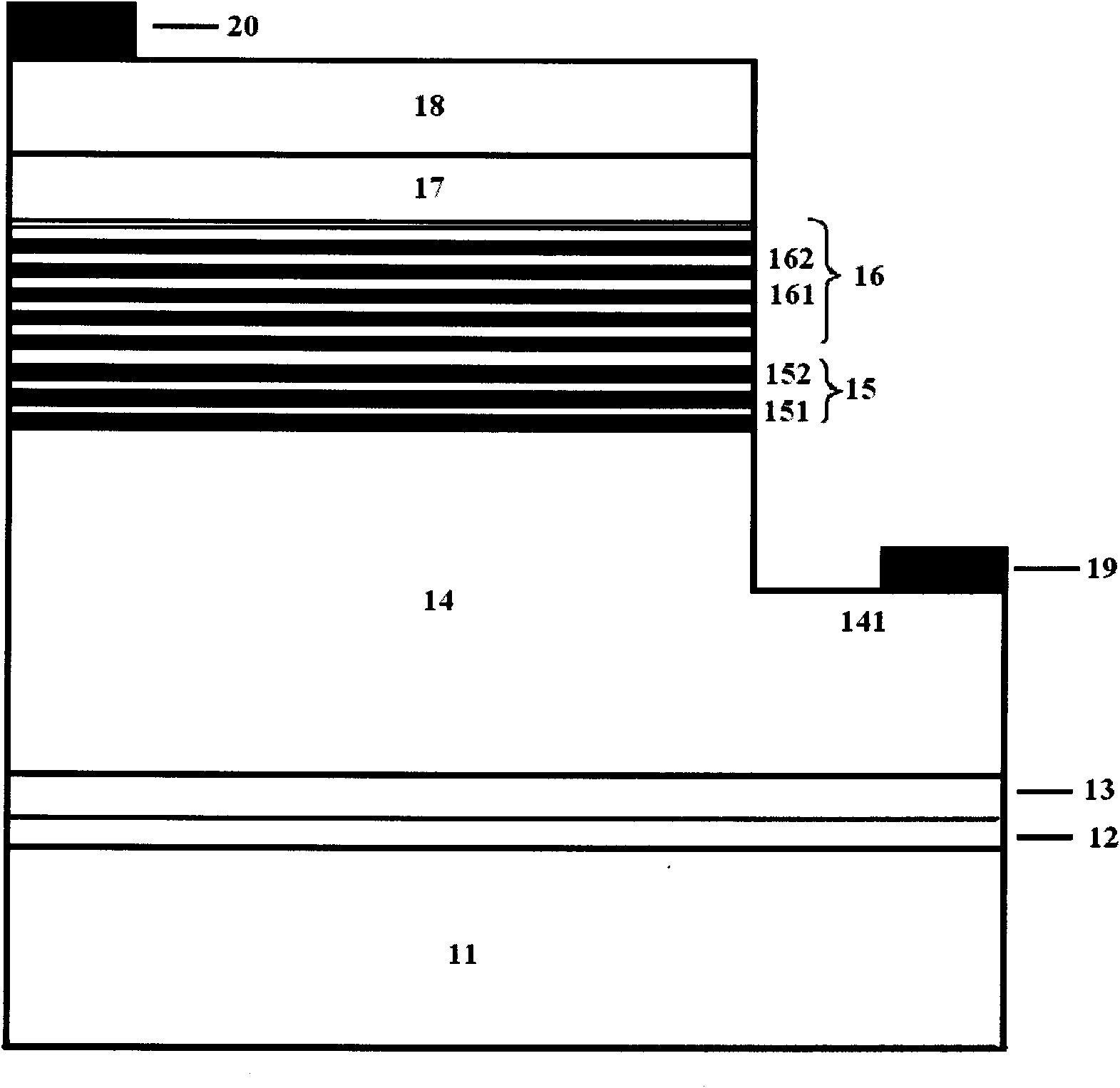
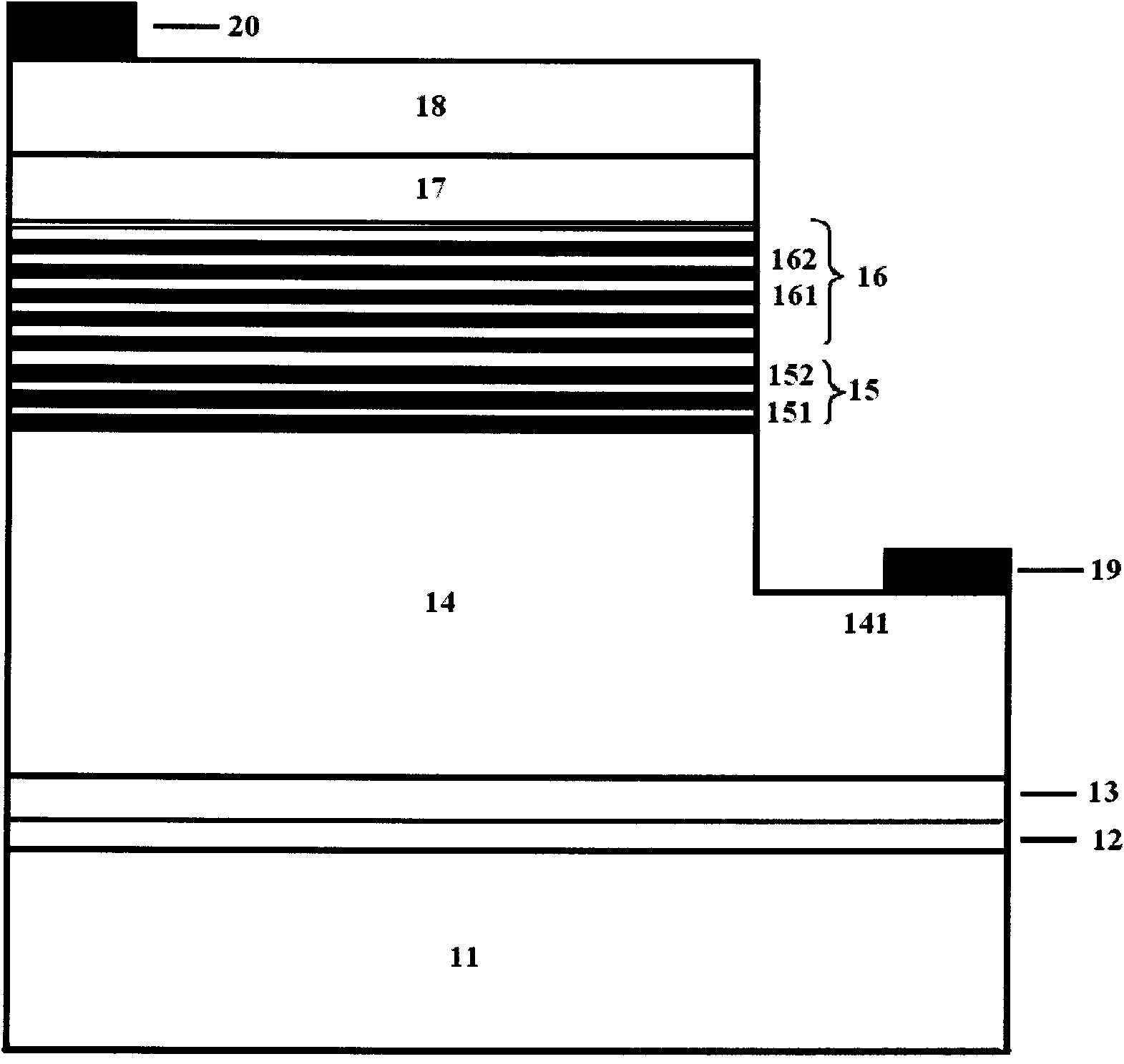
[0024] see figure 1 As shown, the present invention provides a method for manufacturing a modulated doped gallium nitride-based light-emitting diode, the manufacturing process of which is as follows:

[0025] Step 1: Take a substrate 11, and use (0001) to sapphire (Al 2 o 3 ) is the substrate 11, and other materials that can be used for the substrate 11 also include aluminum oxide single crystals on the R-plane or A-plane, 6H-SiC, 4H-SiC, or single crystal oxides whose lattice constants are close to those of nitride semiconductors thing. High-purity NH was used in the preparation 3 As N source, high-purity H 2 and N 2 mixed gas as carrier gas; trimethylgallium or triethylgallium as Ga source, trimethylindium as In source, trimethylaluminum as Al source; n-type dopant is silane, p-type dopant is Magnesium dichloride.

[0026] Step 2: sequentially fabricate a GaN nucleation layer 12 and a GaN buffer layer 13 on the substrate 11 . The growth parameters of the nucleation l...


PUM

PropertyMeasurementUnit
thicknessaaaaaaaaaa

Abstract

The invention relates to a manufacturing method of a modulation-doped gallium nitride series light-emitting diode. The manufacturing method comprises the following steps of: step 1, preparing a substrate; step 2, manufacturing a gallium nitride nucleating layer and a gallium nitride buffer layer in sequence on the substrate; step 3, manufacturing an n-type gallium nitride contact layer on the gallium nitride buffer layer, and taking silane as an n-type doping agent; step 4, manufacturing an n-type current expanding layer, an active luminous layer, a p-type electronic blocking layer and a p-type contact layer in sequence on the upper surface of the n-type contact layer, which is not etched; step 5, etching the upper side of the p-type contact layer downwards with the etching depth reaching into the n-type gallium nitride contact layer by adopting an etching method to so that a platform surface is formed at one side of the n-type gallium nitride contact layer; and step 6, manufacturing a negative electrode on the platform surface of the n-type contact layer; and finally manufacturing a positive electrode on the p-type contact layer.

Description

technical field [0001] The invention relates to a method for doping a gallium nitride (GaN) light-emitting diode, in particular to a method for manufacturing a gallium nitride light-emitting diode modulated and doped with multiple quantum well barrier layers. Background technique [0002] At present, III-V semiconductor optoelectronic materials are known as the third generation semiconductor materials. GaN-based light-emitting diodes have become the focus of industry research because they can produce light-emitting diodes (referred to as "LEDs") of various colors (especially blue or violet light that requires a high energy gap) by controlling the composition of materials. [0003] The epitaxial growth of GaN-based semiconductor materials or devices currently mainly adopts MOCVD technology. In the process of growing nitride semiconductors (GaN, AlN, InN and their alloy nitrides) using MOCVD technology, sapphire is usually used as the substrate for heteroepitaxy because there...

Claims


Application Information

Patent Timeline
Patent Type & Authority Applications(China)
IPC IPC(8): H01L33/00
Inventor 马平王军喜王国宏曾一平李晋闽
Owner INST OF SEMICONDUCTORS - CHINESE ACAD OF SCI
Why Eureka
Try Eureka