Method for evaporating indium tin oxide (ITO)

A technology of evaporation and evaporation rate, applied in vacuum evaporation plating, sputtering plating, ion implantation plating, etc., can solve problems such as insufficient brightness, and achieve improved chip brightness, uniform current expansion, and high light transmittance. Effect

Active Publication Date: 2011-09-21
EPILIGHT TECH
View PDF3 Cites 17 Cited by
  • Summary
  • Abstract
  • Description
  • Claims
  • Application Information

AI Technical Summary

Problems solved by technology

[0002] Light-emitting diodes (LEDs) have the advantages of small size, power saving, and environmental protection. They have been widely used in consumer markets such as display backlight modules, communications, computers, traffic signs, and toys. However, due to the problem of insufficient brightness, they have not been used yet. Widely used in the lighting market

Method used


Image

  • Method for evaporating indium tin oxide (ITO)
  • Method for evaporating indium tin oxide (ITO)
  • Method for evaporating indium tin oxide (ITO)

Examples


Embodiment Construction

[0018] The method for evaporating ITO of the present invention will be described in detail below through specific examples.

[0019] See Figure 4 , the method for evaporation ITO of the present invention mainly comprises the following steps:

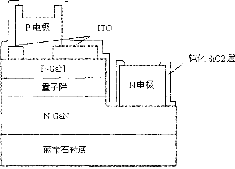
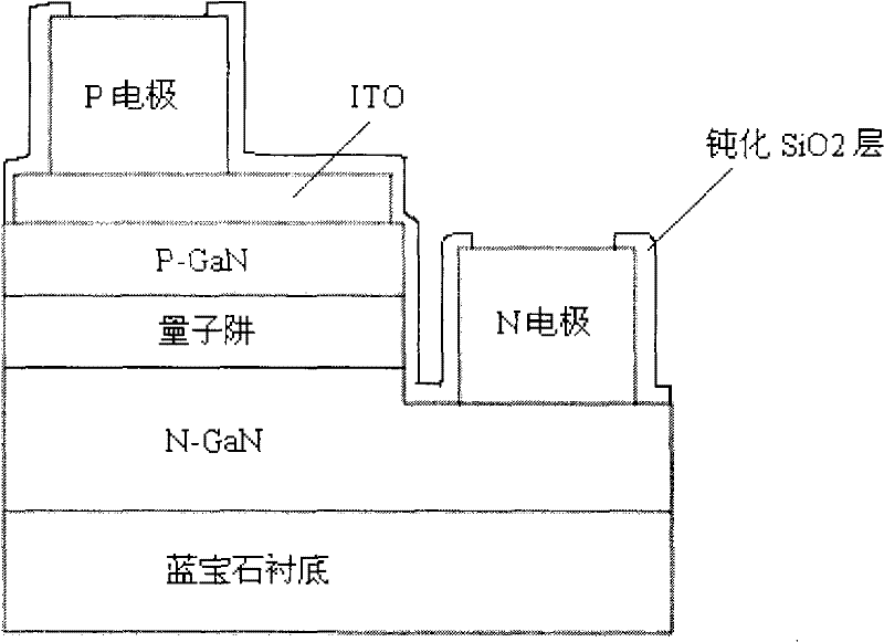
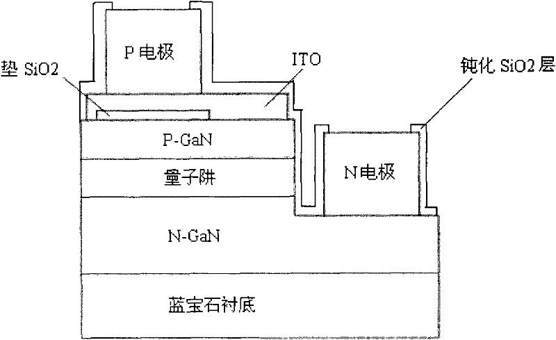
[0020] First, the semiconductor structure to be deposited with ITO (indium tin oxide thin film) is placed on the substrate plate, and the vacuum is evacuated until the vacuum degree of the cavity of the electron beam evaporation machine reaches 5×10 -6 Torr above. In this embodiment, the semiconductor structure is a semiconductor structure for preparing LED chips, which includes a sapphire substrate and a GaN semiconductor layer, wherein the GaN semiconductor layer includes an N-GaN layer, a quantum well, and a P-GaN layer .

[0021] Next, start to rotate the substrate plate, heat it to 240-350° C. and stabilize it for 10-30 minutes.

[0022] Then, open the oxygen valve, and start pre-plating the semiconductor structure when the oxy...


PUM

PropertyMeasurementUnit
transmittivityaaaaaaaaaa

Abstract

The invention provides a method for evaporating indium tin oxide (ITO). The method comprises the following steps: putting a semi-conductor structure on which the ITO is to be evaporated on a wafer-bearing disk; vacuumizing until the vacuum degree of a cavity of a electron beam evaporation machine is above 5*10<-6> Torr, then rotating the wafer-bearing disk, and preheating the wafer-bearing disk to a preset temperature and stabilizing for 10-30 minutes; then opening an oxygen valve, and pre-plating the semi-conductor for 1-5 minutes when oxygen flow is stabilized to a preset flow; and finally, evaporating the ITO at a preset evaporation speed, so that the ITO with a preset thickness is evaporated out on the semi-conductor structure. In the method, the ITO resistance is controlled through controlling oxygen flow, evaporation temperature, ITO thickness and evaporation rate, and simultaneously, the high light transmittance is maintained, so that the ITO resistance is matched with the epitaxial GaN layer, and current is more evenly expanded, thereby effectively improving the brightness of the chip.

Description

technical field [0001] The invention relates to the field of light-emitting diode chip manufacturing, in particular to a method for evaporating ITO. Background technique [0002] Light-emitting diodes (LEDs) have the advantages of small size, power saving, and environmental protection. They have been widely used in consumer markets such as display backlight modules, communications, computers, traffic signs, and toys. However, due to the problem of insufficient brightness, they have not been used yet. Widely used in the lighting market. In order to solve the problem of insufficient brightness of light-emitting diodes, people in the industry are constantly looking for various methods to increase brightness. [0003] ITO is the abbreviation of Indium Tin Oxides in English, which means indium tin oxide. Compared with other transparent semiconductor conductive films, ITO has good chemical stability and thermal stability, and has good adhesion and pattern processing characterist...

Claims


Application Information

Patent Timeline
Patent Type & Authority Applications(China)
IPC IPC(8): H01L33/42C23C14/30C23C14/54
Inventor 李士涛郝茂盛袁根如陈诚
Owner EPILIGHT TECH
Why Eureka
Try Eureka