
Preparation method of GaN substrate

A substrate and thick film technology, used in chemical instruments and methods, semiconductor/solid-state device manufacturing, crystal growth, etc., can solve the problems of GaN substrate material crystal quality, low yield, and high price. Inexpensive, transfer stress distribution, easy to prepare effect

Inactive Publication Date: 2011-09-28
北京燕园中镓半导体工程研发中心有限公司
View PDF2 Cites 27 Cited by
  • Summary
  • Abstract
  • Description
  • Claims
  • Application Information

AI Technical Summary

Problems solved by technology

[0007] The above three methods have high requirements for low-temperature insertion layer, lateral epitaxy technology and other processes, and the process is relatively complicated, which is easily affected by the process and affects the crystal quality of GaN substrate materials. Not high, leading to the fact that the existing GaN substrate has not yet been commercialized, and the price is expensive

Method used


Image

  • Preparation method of GaN substrate
  • Preparation method of GaN substrate
  • Preparation method of GaN substrate

Examples


Embodiment 1

[0027] Embodiment 1. Preparation of c-plane self-supporting GaN substrate:

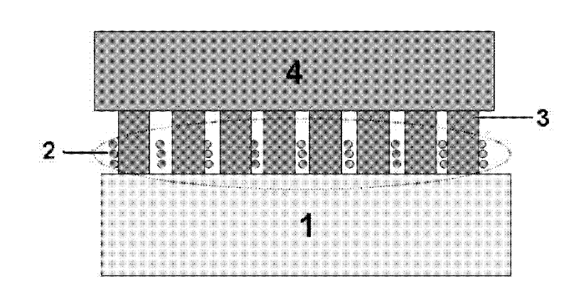
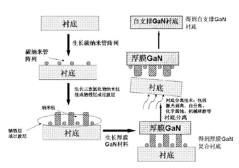
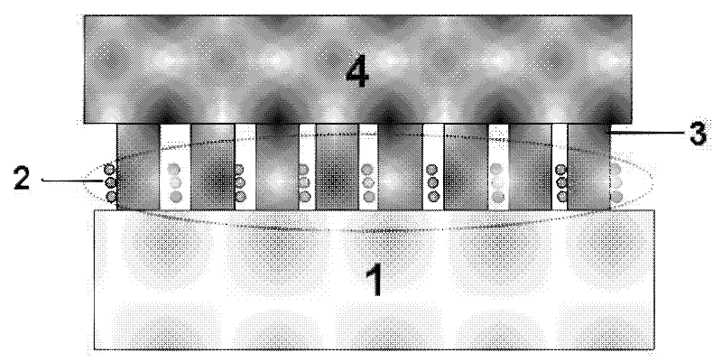
[0028] 1) The substrate can be sapphire, silicon carbide, Si and other substrates, or GaN, AlN, InN or other III-nitride material films grown on sapphire, silicon carbide, Si and other substrates; carbon nanotube arrangement The method is a parallel arrangement along the growth plane, and the arrangement method can be isoperiodic or periodic disordered structure. The carbon nanotubes can be a single carbon nanotube or a cluster of carbon nanotubes in a single-layer or multi-layer Various forms such as: the present embodiment selects the sapphire substrate of c surface, selects the three-layer carbon nanotubes that equiperiodically arranges along the vertical direction of the substrate reference edge; Nanometer; the period is 1-100 microns, preferably 1-10 microns, and 2 microns are used in this embodiment;

[0029] 2) On the above-mentioned substrate covered with carbon nanotubes, a GaN nanocolumn st...

Embodiment 2

[0035] Embodiment 2. Preparation of c-plane GaN thick film substrate:

[0036] 1) The substrate can be sapphire, silicon carbide, Si and other substrates, or GaN, AlN, InN or other III-nitride material films grown on sapphire, silicon carbide, Si and other substrates; carbon nanotube arrangement The method is a parallel arrangement along the growth plane, and the arrangement method can be isoperiodic or periodic disordered structure. The carbon nanotubes can be a single carbon nanotube or a cluster of carbon nanotubes in a single-layer or multi-layer Various forms such as: the present embodiment selects the sapphire substrate of c surface, selects the three-layer carbon nanotubes that equiperiodically arranges along the vertical direction of the substrate reference edge; Nanometer; the period is 1-100 microns, preferably 1-10 microns, and 2 microns are used in this embodiment;

[0037] 2) On the above-mentioned substrate covered with carbon nanotubes, use MOCVD growth technol...

Embodiment 3

[0043] Embodiment 3. Preparation of non-polar a-plane self-supporting GaN or thick film composite substrate:

[0044] 1) The substrate can be r-plane sapphire, silicon carbide, Si and other substrates, or GaN, AlN, InN or other III-nitride material films grown on sapphire, silicon carbide, Si and other substrates; The arrangement of the tubes is a parallel arrangement along the growth plane. The arrangement can be isoperiodic or periodic disordered structure. The carbon nanotubes can be a single carbon nanotube or a cluster of carbon nanotubes and other forms: In this embodiment, the r-plane sapphire substrate is selected, and research shows that a-plane GaN is obtained by epitaxy on the r-plane sapphire. Three-layer carbon nanotubes arranged in the vertical direction along the reference edge of the substrate are selected for use; the diameter of the carbon nanotubes is 1-100 nanometers, and 20 nanometers are used in this embodiment; the period is 1-100 microns, preferably 1-1...


PUM

PropertyMeasurementUnit
thicknessaaaaaaaaaa
thicknessaaaaaaaaaa
thicknessaaaaaaaaaa

Abstract

The invention provides a preparation method of a GaN substrate, belonging to the field of preparation of photoelectronic devices. The key points of the preparation method different from the prior art are as follows: a transition layer formed by carbon nano tubes and GaN, InGaN, AlGaN, AlN or InN nano columns is formed on the epitaxial growth surface of a substrate (such as Si, sapphire and SiC and the like), then a thick film GaN grows, the thick-film GaN substrate is obtained or a self-support GaN substrate is obtained by a substrate removing process or a self-separation process. In the invention, the preparation method is simple, the process condition is easily controlled, the price is low, different substrates can be selected and multiple substrate separating technologies also can be supported.

Description

technical field [0001] The invention relates to a preparation technology of a GaN substrate, which belongs to the field of preparation of optoelectronic devices. Background technique [0002] The lattice mismatch and thermal mismatch between the sapphire or silicon carbide substrates widely used at present and the GaN material are relatively large, resulting in a decline in the quality of the GaN material and its devices. The technology of preparing self-supporting GaN or composite thick-film GaN substrates by using the epitaxy method combined with HVPE and MOCVD or MBE has always been very important for GaN high-power LEDs, lasers and other high-performance optoelectronic devices. [0003] Due to the large lattice mismatch and thermal mismatch between substrates such as sapphire or silicon carbide and GaN materials, the preparation of GaN substrates has always been affected by large residual stress, bending or even cracking of epitaxial wafers and cannot be widely used. Th...

Claims


Application Information

Patent Timeline
Patent Type & Authority Applications(China)
IPC IPC(8): H01L21/20H01L33/00H01S5/00C30B25/02C30B29/38
Inventor 于彤军龙浩张国义吴洁君贾传宇杨志坚
Owner 北京燕园中镓半导体工程研发中心有限公司
Learn More