Method for detecting gigahertz single photon with low time jitter and low noise

A single-photon detection and time jitter technology, applied in instruments and other directions, can solve the problems of large time jitter, difficult to meet the requirements of ranging, and reduce the amplitude of the avalanche signal, so as to maintain the amplitude and integrity, reduce the time jitter, and maintain the avalanche signal. Amplitude effect

Active Publication Date: 2011-11-02
EAST CHINA NORMAL UNIVERSITY
5 Cites 11 Cited by

AI-Extracted Technical Summary

Problems solved by technology

However, while filtering the noise, the corresponding spectral components of the avalanche signal are also filtered out, which destroys the integrity of the avalanche signal. Multiple filtering will not only reduce the amplitude of the avalanche signal, but also increase the t...

Abstract

The invention relates to the field of quantum secret communication and weak infrared light detection in the technical field of optical fiber communication, in particular to a method for detecting a gigahertz high-speed near infrared single photon with low time jitter and low noise. A control circuit related to the method consists of a signal detection circuit, a noise suppressing circuit and a signal processing circuit, wherein the noise suppressing circuit is used for extracting an avalanche electric signal by the following steps of: dividing a sine signal of gigahertz into two paths; loading one path serving as a gate signal on an avalanche photoelectric diode; transmitting a response output signal of the avalanche photoelectric diode to a low-pass filter; attenuating the other path of sine signal to an amplitude which is same as that of the response signal of the avalanche photoelectric diode passing through the low-pass filter; and transmitting the other path of sine signal to a balance circuit for balancing with the response signal of the avalanche photoelectric diode passing through the low-pass filter to remove spike noise and extract the avalanche electric signal. In the method, the spike noise is removed in a way of combining low-pass filtering with the balance circuit, so that the avalanche signal is extracted, higher detection efficiency is achieved, and the time jitter is controlled within dozens of picoseconds.

Application Domain

Technology Topic

Image

  • Method for detecting gigahertz single photon with low time jitter and low noise
  • Method for detecting gigahertz single photon with low time jitter and low noise
  • Method for detecting gigahertz single photon with low time jitter and low noise

Examples

  • Experimental program(1)

Example Embodiment

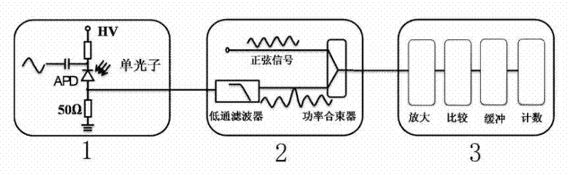
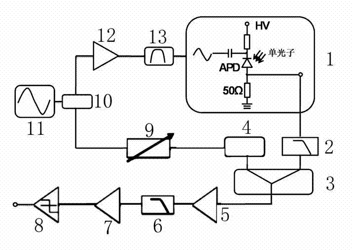
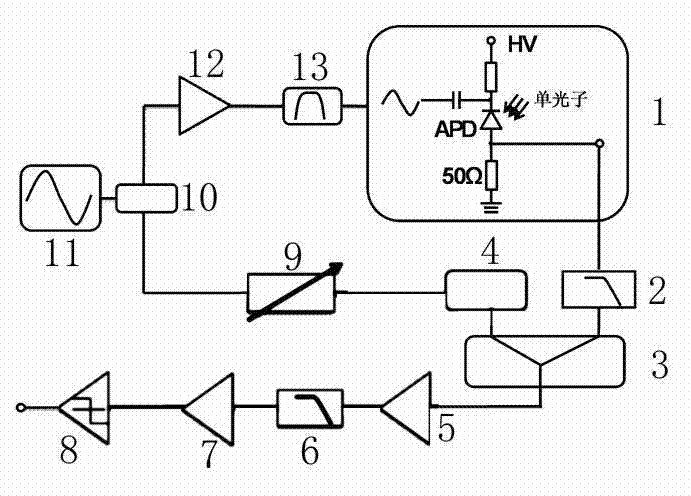
[0017] Example: such as Figure 1-2 As shown, the numbers 1-13 respectively indicate: detection circuit 1, noise suppression circuit 2, signal processing circuit 3, phase shifter 4, radio frequency amplifier 5, low pass filter 6, radio frequency amplifier 7, comparator 8, adjustable attenuation Detector 9, power splitter 10, sinusoidal signal generator 11, high power amplifier 12, band pass filter 13.
[0018] Such as figure 1 As shown, the detection circuit converts the single-photon signal into an electrical signal through the APD. In the converted electrical signal, the avalanche signal is annihilated in the spike noise caused by the capacitive effect of the APD, and the avalanche signal is extracted by the noise suppression circuit. The noise suppression circuit is composed of a low-pass filter and a balance circuit. The signal is first passed through the low-pass filter and then balanced with the attenuated sinusoidal signal to remove noise and extract the avalanche signal. Finally, the extracted avalanche signal is converted into a digital signal through a signal processing circuit, and the count is output.
[0019] The specific analog circuit principle of this embodiment is as follows figure 2 Shown. The sinusoidal signal generator 11 generates a sinusoidal signal with a repetition frequency of ω, which is divided into two equal parts by the power splitter 10. One of the sinusoidal signals is amplified by the high-power amplifier 12, and then loaded on the APD as a gate pulse after passing through a band-pass filter 13. The amplitude of the sinusoidal signal generated by the sinusoidal signal generator is limited. After a high-power amplifier 12, the amplitude adjustment range of the sinusoidal signal is larger, which can fully meet the gate pulse amplitude required by the optimal operating point of the detector. After passing through the high power amplifier 12, bypass noise and resonance noise of other frequencies will be generated, which are filtered out by a bandpass filter 13 with a center frequency of ω. Adjust the bias voltage at both ends of the APD to work in avalanche mode to convert the optical signal into an avalanche signal. The avalanche signal output by the APD is annihilated in the spike noise, and the spike noise is filtered through a low-pass filter 2 with a cut-off frequency of ω. The filtered APD output signal is input to the power combiner 3 for balance. The reference signal of the balance circuit is an attenuated sinusoidal signal, the amplitude of which is the same as the filtered spike noise through the adjustable attenuator 9, and the phase difference between the two is 180° through the phase shifter 4. After the power combiner 3, the peak noise is basically reduced to the thermal noise level, which can be ignored, and the avalanche signal is extracted. The avalanche signal amplified by the two radio frequency amplifiers 5 and 7 is converted into a digital signal after the comparator 8 is buffered, and then sent to a counter for counting to realize single photon detection. Adding a low-pass filter 6 with a cutoff frequency of 2ω between the two radio frequency amplifiers 5 and 7 can prevent the crosstalk between the two amplifiers 5 and 7 from affecting the signal.
[0020] The present invention is composed of a signal detection circuit 1, a noise suppression circuit 2, and a signal processing circuit 3. The signal detection circuit 1 uses the APD to convert the detected optical signal into an avalanche electrical signal and sends it to the noise suppression circuit 2. The noise suppression circuit 2 suppresses the spike noise, extracts the avalanche signal, and finally the extracted avalanche signal enters the signal processing circuit 3. Convert analog signals into digital signals for counting. Due to the capacitive effect of the APD, while converting the optical signal into an avalanche electrical signal, spike noise is also generated. By using a low-pass filter 2, the noise can be filtered out to extract the avalanche signal. However, only one low-pass filter 2 is used, and the peak noise suppression ratio is not enough. Therefore, the sinusoidal gate signal is divided into two channels, and the amplitude of one channel is attenuated to the same amplitude as the low-pass filtered peak noise, and then sent to the balance circuit and After low-pass filtering, the spike noise is balanced and the avalanche signal is extracted. The signal processing circuit is composed of signal amplification, comparison, buffering, and counting. The avalanche signal enters the comparator 8 after being amplified, and the signal from the comparator 8 enters the counter to count after being buffered.

PUM

no PUM

Description & Claims & Application Information

We can also present the details of the Description, Claims and Application information to help users get a comprehensive understanding of the technical details of the patent, such as background art, summary of invention, brief description of drawings, description of embodiments, and other original content. On the other hand, users can also determine the specific scope of protection of the technology through the list of claims; as well as understand the changes in the life cycle of the technology with the presentation of the patent timeline. Login to view more.

Similar technology patents

Optical delay line interferometer

ActiveUS20100119189A1High symmetryImprove signal-to-noise ratioLight demodulationElectromagnetic receiversPhysicsPolarization coupling
Owner:NIPPON TELEGRAPH & TELEPHONE CORP

Classification and recommendation of technical efficacy words

  • Reduce time jitter
  • Improve signal-to-noise ratio

Device for generating Nyquist optical pulse based on ultra-broadband optical frequency comb

ActiveCN104330940AGood time stabilityReduce time jitterLight demodulationPhase shiftedOptical coupler
Owner:INST OF SEMICONDUCTORS - CHINESE ACAD OF SCI

Single-ended negative feedback charge pump for delay-locked loop

ActiveCN107565961ASuppressing Current Mismatch IssuesReduce time jitterPulse automatic controlIntegrated circuitDelay-locked loop
Owner:青岛展诚科技有限公司

Superconducting nanowire single-photon detection system with tapered transmission line

InactiveCN110793631AReduce time jitterIncrease count ratePhotometry electrical circuitsTransmission linePhoton detection
Owner:SHANGHAI INST OF MICROSYSTEM & INFORMATION TECH CHINESE ACAD OF SCI

Plasma display panel

InactiveCN1937139AReduce time jitterIncrease the number of dischargesSustain/scan electrodesAuxillary electrodesAuxiliary electrodeDischarge efficiency
Owner:NANJING LG TONGCHUANG COLOR DISPLAYS SYST CO LTD

Magnetic tape, its cleaning method, and optical servotrack forming/cleaning apparatus

InactiveUS7803471B1Improve signal-to-noise ratioDecreasing rate of fluctuationMagnetic materials for record carriersReconditioning/cleaning record carriersReflectivityMaximum rate
Owner:FUJIFILM CORP

Hyper-spectral imaging methods and devices

InactiveUS20050270528A1Improve signal to noise ratioSmall bandwidthRadiation pyrometrySpectrum generation using diffraction elementsSpectral imagingLight spectrum
Owner:PLAIN SIGHT SYST
Why Eureka
Try Eureka