
Method for improving topography and electrical properties of ZnO (zinc oxide) thin film

A technology of electrical properties and thin films, applied in the field of solar cells, can solve problems such as reducing the resistivity of ZnO thin films, and achieve the effects of improving electrical conductivity, improving electrical conductivity, and eliminating edges and corners.

Active Publication Date: 2011-11-09
NANKAI UNIV
View PDF3 Cites 4 Cited by
  • Summary
  • Abstract
  • Description
  • Claims
  • Application Information

AI Technical Summary

Problems solved by technology

[0004] The purpose of the present invention is to provide a method for improving the morphology and electrical properties of ZnO films for the problems of the edges and sharp peaks and the reduction of ZnO film resistivity in the textured ZnO films directly prepared in the prior art. The method adopts low-cost Combination of Ultrasonic Spray Pyrolysis (USP) and Magnetron Sputtering to Prepare Textured ZnO Thin Films

Method used


Image

  • Method for improving topography and electrical properties of ZnO (zinc oxide) thin film
  • Method for improving topography and electrical properties of ZnO (zinc oxide) thin film
  • Method for improving topography and electrical properties of ZnO (zinc oxide) thin film

Examples


Embodiment 1

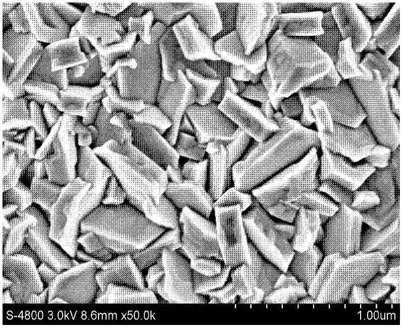
[0032] Using the USP method, zinc acetate is used as Zn source, and indium acetate is used as doped indium source. Water and absolute ethanol were mixed at a ratio of 1:3 as a solvent, and zinc acetate was configured as a 0.2 mol / L solution, and indium acetate was added according to Zn / In=1at.%, and 10vol.% glacial acetic acid was added at the same time. Eagle 2000 glass was used as the substrate. The growth temperature was 470°C. Compressed air was used as the carrier gas, and the surface morphology of the prepared 1at.% In-doped IZO film was as follows figure 1 As shown, its root mean square surface roughness is 62.4nm. More obvious edges and peaks can be seen.

[0033]The AZO film was prepared on the above 1at.% In-doped IZO film by intermediate frequency magnetron sputtering, using a zinc-aluminum alloy target with a mass ratio of 2w.%, at a growth temperature of 280°C, and a reaction gas of high-purity O 2 , the flow rate is 1.5 sccm, and the AZO thin film of 300 nm i...

Embodiment 2

[0035] Using the USP method, zinc acetate is used as Zn source, and indium acetate is used as doped indium source. Water and absolute ethanol were mixed at a ratio of 1:3 as a solvent, and zinc acetate was configured as a 0.2mol / L solution, and indium acetate was added according to Zn / In=1at.%, and 10vol.% glacial acetic acid was added at the same time. Eagle 2000 glass was used as the substrate. The growth temperature was 470°C. Compressed air was used as carrier gas to prepare 1 at.% In-doped IZO film.

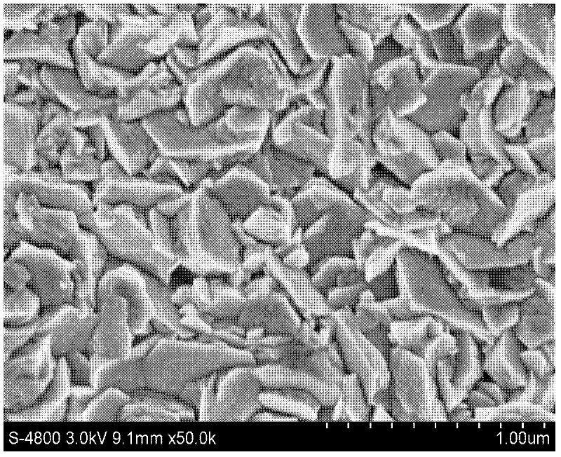
[0036] AZO film was prepared on 1at.% In-doped IZO film by intermediate frequency magnetron sputtering method, using a zinc-aluminum alloy target with a mass ratio of 2w.%, at a growth temperature of 280°C, and a reaction gas of high-purity O 2 , the flow rate is 1.5 sccm, and the AZO thin film of 500 nm is prepared by controlling the growth time for 50 min. The surface morphology of the obtained ZnO thin film composite film is as follows: Figure 5 ;and figure 1 For co...

Embodiment 3

[0038] Using the USP method, zinc acetate is used as Zn source, and indium acetate is used as doped indium source. Water and absolute ethanol were mixed at a ratio of 1:3 as a solvent, and zinc acetate was configured as a 0.2mol / L solution, and indium acetate was added according to Zn / In=1at.%, and 10vol.% glacial acetic acid was added at the same time. Eagle 2000 glass was used as the substrate. The growth temperature was 470°C. Compressed air was used as carrier gas to prepare 1 at.% In-doped IZO film.

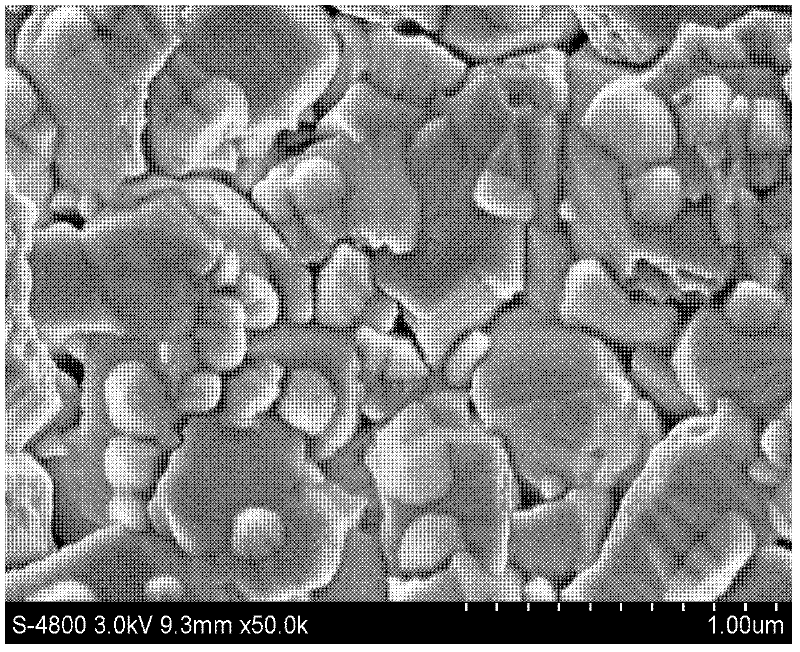
[0039] AZO film was prepared on 1at.% In-doped IZO film by intermediate frequency magnetron sputtering method, using a zinc-aluminum alloy target with a mass ratio of 2w.%, at a growth temperature of 280°C, and a reaction gas of high-purity O 2 , the flow rate is 1.5 sccm, and the AZO thin film of 1000 nm is prepared by controlling the growth time for 100 min. The surface morphology of the obtained ZnO thin film composite film is as follows: Figure 7 ;and figure 1 For ...


PUM

PropertyMeasurementUnit
thicknessaaaaaaaaaa
surface roughnessaaaaaaaaaa
electrical resistivityaaaaaaaaaa

Abstract

The invention provides a method for improving topography and electrical properties of a ZnO (zinc oxide) thin film. The method comprises the following steps: 1) by taking zinc acetate as a Zn source, acetic acid indium as a doped indium source and a mixed liquor of water and absolute ethyl alcohol as a solvent, adding the zinc acetate to the solvent to obtain a precursor mixed liquor, adding glacial acetic acid to the precursor mixed liquor, and by taking airs as a carrier gas, preparing an indium-doped ZnO thin film with a triangle topography on a glass substrate by using an ultrasonic spraypyrolysis method; and 2) by taking aluminum-zinc alloy as target materials, preparing an aluminum-doped ZnO thin film on the indium-doped ZnO thin film by using a magnetron sputtering method. The method has the advantages that the prepared indium-doped ZnO thin film or the aluminum-doped ZnO thin film is of a conical textured topography without edges and sharp peaks, thus having stronger scattering effect on incident lights; and meanwhile, the ZnO thin film prepared by the sputtering technique has the characteristic of low resistivity, so the conductive properties of the ZnO thin film can be obviously improved.

Description

【Technical field】 [0001] The invention belongs to the technical field of solar cells, in particular to a method for improving the morphology and electrical properties of a ZnO thin film. 【Background technique】 [0002] Transparent conductive oxide films (TCOs) are essential electrode materials for thin-film solar cells. TCO with textured surface is an important basis for forming silicon thin film solar cells with light trapping structure. The introduction of the light-trapping structure can increase the optical path of the incident light and enhance the light absorption of the cell, which is particularly important for improving the performance of the device. In recent years, due to the SnO 2 Thin films have good electrical and optical properties and are widely used as transparent conductive films for solar cells. However, the optical properties of this material deteriorate due to the reduction of Sn in a hydrogen plasma atmosphere, which limits its application as a transp...

Claims


Application Information

Patent Timeline
Patent Type & Authority Applications(China)
IPC IPC(8): H01L31/18C23C14/08C23C14/35
CPCY02P70/50
Inventor 张晓丹赵颖焦宝臣魏长春
Owner NANKAI UNIV
Learn More