Controlled silicon for large-size silicon chip employing plastic entity package and packaging process thereof

A silicon chip, large-scale technology, used in the packaging field of semiconductor devices, can solve the problems of large plastic curing stress and thermal stress of silicon chips, power limitation of device products, low packaging qualification rate and reliability, etc., and achieve uniform current distribution. , Reduce the probability of hot spots, the effect of simple structure

Active Publication Date: 2011-11-23
JIANGSU JIEJIE MICROELECTRONICS
View PDF6 Cites 3 Cited by
  • Summary
  • Abstract
  • Description
  • Claims
  • Application Information

AI Technical Summary

Problems solved by technology

[0003] At present, the chip size of the silicon controlled rectifier in the plastic physical package generally does not exceed 7×7mm. The main factor limiting the chip size of the plastic physical package is that the expansion coefficients of the three materials, the chip, the copper base plate, and the plastic encapsulant, are greatly different. Silicon chips packaged into products will have large plastic curing stress and thermal stress, which is extremely detrimental to the reliability of the product, so the packaging pass rate and reliability of this type of product are relatively low
However, because products with plastic physical packaging are more convenient to install and connect electrodes in use, some people in the industry have been pursuing physical packaging of larger chips. The addition of molybdenum sheet, which has a similar expansion coefficient to single crystal silicon, is beneficial to reduce the stress caused by the difference in expansion coefficient between the silicon chip and the copper base plate, and the plastic packaging compound. However, due to the addition of two layers, the thermal conductivity is relatively small and the resistivity is relatively large. The metal sheet and two layers of solder will significantly increase the on-state voltage drop and thermal resistance of the device, which will limit the power of the device to a certain extent.

Method used


Image

  • Controlled silicon for large-size silicon chip employing plastic entity package and packaging process thereof
  • Controlled silicon for large-size silicon chip employing plastic entity package and packaging process thereof
  • Controlled silicon for large-size silicon chip employing plastic entity package and packaging process thereof

Examples


Embodiment 1

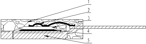
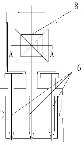
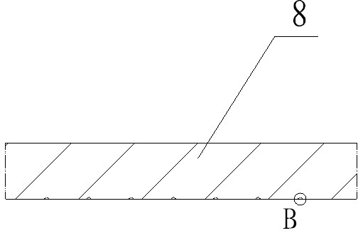
[0035] like Figures 1 to 6 As shown, a kind of large-size silicon chip of the present invention adopts the silicon controlled rectifier of plastic entity package, comprises copper base plate 5 and pin 6, is welded with silicon chip 3 by lead-tin solder 4 on copper base plate 5, welds on silicon chip 3 There are aluminum wire inner leads 2, and the outside of the aluminum wire inner leads 2 is plastic-sealed by a plastic sealing compound 1. The plastic sealing compound 1 is made of a low-stress plastic sealing compound. There are plastic grooves 7 between the pins 6, and a drainage groove 8 is opened on the copper base plate 5. The drainage groove 8 is square, and the section of the drainage groove 8 is V-shaped. Five aluminum wire inner leads 2 are welded on the silicon chip 3, and each aluminum wire inner lead 2 is pressed with two solder joints 9 on the silicon chip 3. The upper surface of the chip 3 is covered with a thickened Al layer with a thickness of 18 μm, and the lo...

Embodiment 2

[0037] like Figures 1 to 6 As shown, a kind of large-size silicon chip of the present invention adopts the silicon controlled rectifier of plastic entity package, comprises copper base plate 5 and pin 6, is welded with silicon chip 3 by lead-tin solder 4 on copper base plate 5, welds on silicon chip 3 There are aluminum wire inner leads 2, and the outside of the aluminum wire inner leads 2 is plastic-sealed by a plastic sealing compound 1. The plastic sealing compound 1 is made of a low-stress plastic sealing compound. There are plastic grooves 7 between the pins 6, and a drainage groove 8 is opened on the copper base plate 5. The drainage groove 8 is circular, and the section of the drainage groove 8 is V-shaped. Five aluminum wire inner leads 2 are welded on the silicon chip 3, and each aluminum wire inner lead 2 is pressed with two solder joints 9 on the silicon chip 3. The upper surface of the silicon chip 3 is covered with a thickened Al layer with a thickness of 20 μm, ...

Embodiment 3

[0039] like Figures 1 to 6 As shown, a kind of large-size silicon chip of the present invention adopts the silicon controlled rectifier of plastic entity package, comprises copper base plate 5 and pin 6, is welded with silicon chip 3 by lead-tin solder 4 on copper base plate 5, welds on silicon chip 3 There are aluminum wire inner leads 2, and the outside of the aluminum wire inner leads 2 is plastic-sealed by a plastic sealing compound 1. The plastic sealing compound 1 is made of a low-stress plastic sealing compound. There are plastic grooves 7 between the pins 6, and a drainage groove 8 is opened on the copper base plate 5. The drainage groove 8 is in the shape of a square plus a diagonal line, and the section of the drainage groove 8 is V-shaped. There are five aluminum wire inner leads 2 welded on the silicon chip 3, and each aluminum wire inner lead 2 is pressed on the silicon chip 3 with two Solder spot 9, the upper surface of the silicon chip 3 is covered with a thick...


PUM

PropertyMeasurementUnit
thicknessaaaaaaaaaa
thicknessaaaaaaaaaa
thicknessaaaaaaaaaa

Abstract

The invention relates to a controlled silicon for a large-size silicon chip employing a plastic entity package and a packaging process for the controlled silicon. The controlled silicon comprises a copper substrate and pins; a silicon chip is welded on the copper substrate through a lead-tin solder; an aluminum wire internal lead is welded on the silicon chip; the aluminum wire internal lead is plastically packaged through a plastic material; and a plastic groove is formed between the pins. The invention also relates to a process for packaging the controlled silicon for the large-size siliconchip employing the plastic entity package. The method comprises the following steps of: sintering, cleaning, welding, packaging, cutting ribs and testing. The invention has the advantages that: the process is simple and has the advantages of low thermal resistance and low state voltage drop, and the product reliability is improved.

Description

technical field [0001] The invention relates to a thyristor in which a large-size silicon chip is encapsulated by a plastic entity. [0002] The invention also relates to a packaging technology of a thyristor in which a large-size silicon chip is packaged with a plastic entity, and belongs to the technical field of packaging of semiconductor devices. Background technique [0003] At present, the chip size of the silicon controlled rectifier in the plastic physical package generally does not exceed 7×7mm. The main factor limiting the chip size of the plastic physical package is that the expansion coefficients of the three materials, the chip, the copper base plate, and the plastic encapsulant, are greatly different. Silicon chips packaged into products will have large plastic curing stress and thermal stress, which is extremely detrimental to the reliability of the product, so the packaging pass rate and reliability of this type of product are relatively low. However, becaus...

Claims


Application Information

Patent Timeline
Patent Type & Authority Applications(China)
IPC IPC(8): H01L23/28H01L23/488H01L21/56H01L21/60
CPCH01L2924/01074H01L2224/32245H01L2924/01014H01L2924/10253H01L2924/01042H01L2224/48472H01L24/32H01L2224/73265H01L2924/01005H01L2924/01082H01L2224/49111H01L24/45H01L2924/01013H01L2924/15747H01L2924/0105H01L2924/014H01L2924/01023H01L24/49H01L2924/01029H01L2924/01047H01L2224/48247H01L2224/45124H01L2924/01006H01L2924/01033H01L2224/4846H01L2224/0603H01L2924/351H01L24/73H01L2924/181H01L2224/49H01L2224/45H01L2224/29111H01L2224/83801H01L2924/00012H01L2924/00014H01L2924/00
Inventor 王琳吴家健李攀
Owner JIANGSU JIEJIE MICROELECTRONICS
Why Eureka
Try Eureka