Production system of silicon substrate liquid crystal display screen and production method thereof

A silicon-based liquid crystal and production system technology, applied in the direction of optics, instruments, electrical components, etc., can solve the problems of silicon wafer and glass deformation, expensive process equipment, difficult alignment film thickness, etc., to improve assembly quality, reduce costs, The effect of reducing the degree of pollution

Inactive Publication Date: 2012-01-04
SHENZHEN YANGTZE LIVETECH
View PDF8 Cites 15 Cited by
  • Summary
  • Abstract
  • Description
  • Claims
  • Application Information

AI Technical Summary

Problems solved by technology

[0006] The disadvantage of this method is: vacuum plating SiO 2 The process equipment related to the alignment film is expensive, and when the thickness of the alignment film is required to be less than 50nm, SiO 2 The thickness of the alignment film is difficult to achieve a deviation of no more than ±10%; the deviation is very large when using the method of aligning the gap between the indium tin oxide glass and the silicon substrate itself, and it is almost useless in mass production; using heat-cured frame glue, usually Stable baking at about 200 degrees is required to cure the frame glue, which may easily cause deformation differences between silicon wafers and glass, thereby affecting the quality of silicon-based LCD screens; in addition, the process statement is simple, and detailed descriptions of process details are not provided for convenience. Production is practical, and thus lacks practical value

Method used


Image

  • Production system of silicon substrate liquid crystal display screen and production method thereof
  • Production system of silicon substrate liquid crystal display screen and production method thereof
  • Production system of silicon substrate liquid crystal display screen and production method thereof

Examples


Embodiment 1

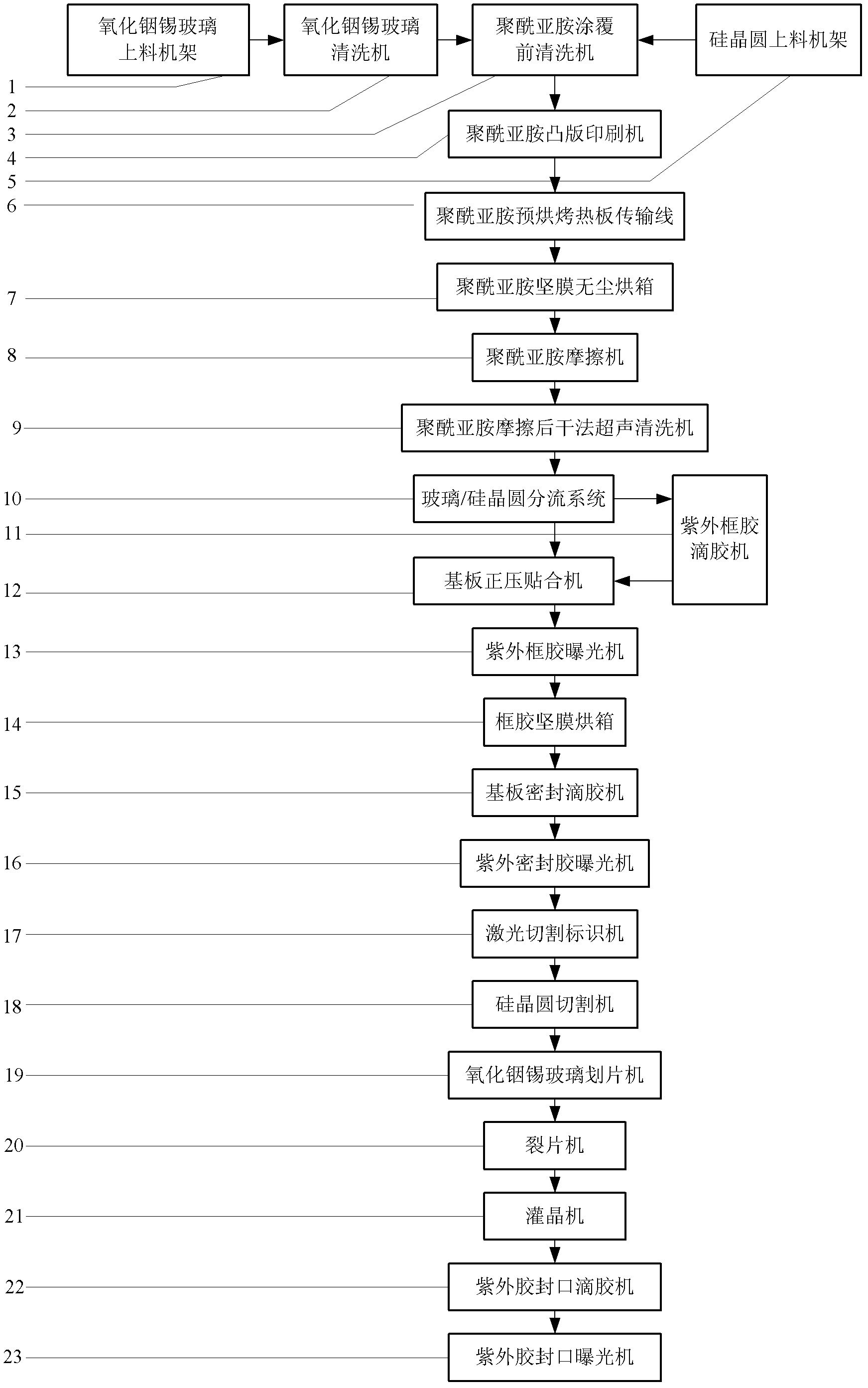
[0063] (1) Substrate cleaning step: the indium tin oxide glass 40 is initially cleaned in the indium tin oxide glass cleaning machine 2, and at least one piece of the indium tin oxide glass 40 that has undergone preliminary cleaning is alternated with at least one piece of the silicon wafer 24 Transported into the cleaning machine 3 before the polyimide coating to complete the cleaning; (2) the cleaned indium tin oxide glass 40 and the silicon wafer 24 are sequentially coated, dried, rubbed, and dry ultrasonically cleaned; Covering polyimide film is carried out in polyimide letterpress printing machine 4, drying can be carried out in polyimide hard film dust-free oven 7, rubbing polyimide film is carried out in polyimide rubbing machine 8 The dry ultrasonic cleaning of the polyimide film is carried out in a dry ultrasonic cleaning machine 9; the thickness of the polyimide film coated on at least one piece of indium tin oxide glass and at least one piece of the silicon wafer is ...

Embodiment 2

[0072] (1) Substrate cleaning step: the indium tin oxide glass 40 is initially cleaned in the indium tin oxide glass cleaning machine 2, and at least one piece of the indium tin oxide glass 40 that has undergone preliminary cleaning is alternated with at least one piece of the silicon wafer 24 Transported into the cleaning machine 3 before the polyimide coating to complete the cleaning; (2) the cleaned indium tin oxide glass 40 and the silicon wafer 24 are sequentially coated, dried, rubbed, and dry ultrasonically cleaned; Covering polyimide film is carried out in polyimide letterpress printing machine 4, drying can be carried out in polyimide hard film dust-free oven 7, rubbing polyimide film is carried out in polyimide rubbing machine 8 The dry ultrasonic cleaning of the polyimide film is carried out in a dry ultrasonic cleaning machine 9; the thickness of the polyimide film coated on at least one piece of indium tin oxide glass and at least one piece of the silicon wafer is ...

Embodiment 3

[0081] (1) Substrate cleaning step: the indium tin oxide glass 40 is initially cleaned in the indium tin oxide glass cleaning machine 2, and at least one piece of the indium tin oxide glass 40 that has undergone preliminary cleaning is alternated with at least one piece of the silicon wafer 24 Transported into the cleaning machine 3 before the polyimide coating to complete the cleaning; (2) the cleaned indium tin oxide glass 40 and the silicon wafer 24 are sequentially coated, dried, rubbed, and dry ultrasonically cleaned; Covering polyimide film is carried out in polyimide letterpress printing machine 4, drying can be carried out in polyimide hard film dust-free oven 7, rubbing polyimide film is carried out in polyimide rubbing machine 8 The dry ultrasonic cleaning of the polyimide film is carried out in a dry ultrasonic cleaning machine 9; the thickness of the polyimide film coated on at least one piece of indium tin oxide glass and at least one piece of the silicon wafer is ...


PUM

PropertyMeasurementUnit
thicknessaaaaaaaaaa
depthaaaaaaaaaa
thicknessaaaaaaaaaa

Abstract

The invention discloses a production system of a silicon substrate liquid crystal display (LCD) screen and a production method thereof. The method comprises the following steps: (1) substrate cleaning: alternatively transferring indium-tin-oxide glass and silicon wafer into a cleaning machine before coating polyimide for completing cleaning; (2) successively coating, drying, rubbing and carrying out dry-method ultrasonic cleaning on the cleaned indium-tin-oxide glass and silicon wafer; (3) sending the cleaned indium-tin-oxide glass and silicon wafer to a glass/silicon wafer split system, transferring the indium-tin-oxide glass to an ultraviolet glue framing and dropping machine, carrying out silicon substrate LCD screen fit processing on the silicon wafer and the indium-tin-oxide glass which is coated with pattern framing flue and processed on the indium-tin-oxide glass, and then completing glue-framing exposure and solidification; (4) successively carrying out glue-framing resolidification, sealing and sealing glue solidification processing on the silicon substrate LCD exposed by glue framing; and (5) irrigating crystal to the silicon substrate LCD screen subjected to the solidification processing of sealing glue to obtain the reflection-type LCD screen. By adopting the method, the assembling quality of the silicon substrate LCD screen can be improved.

Description

technical field [0001] The invention relates to a production line equipment structure and a production method of a liquid crystal display with a silicon-based chip as a substrate, in particular to a silicon-based liquid crystal screen production line structure and a process flow method thereof. Background technique [0002] Liquid Crystal on Silicon (LCOS for short) display technology is a reflective new type of display technology that organically combines Liquid Crystal Display (LCD for short) technology and complementary metal oxide semiconductor (CMOS for short) integrated circuit technology. display technology. First, use CMOS device technology on the silicon wafer to make a silicon-based liquid crystal chip with reflective electrodes for each row or column of pixels, and then bond the silicon-based liquid crystal chip with a glass substrate with a transparent electrode at an appropriate distance, and place it on the silicon wafer. The liquid crystal material is poured ...

Claims


Application Information

Patent Timeline
Patent Type & Authority Applications(China)
IPC IPC(8): G02F1/1333H01L21/00
Inventor 代永平范伟董续怀范义
Owner SHENZHEN YANGTZE LIVETECH
Why Eureka
Try Eureka