Nanometer level polishing solution and preparation method thereof

A kind of polishing liquid and nano-scale technology, applied in the direction of polishing composition containing abrasives, etc., can solve the problems of difficult processing of dispersion properties, insufficient performance, loss of nano-diamonds, etc., to achieve small overall size deformation and complete wafer structure , easy to store effects

Active Publication Date: 2012-01-11
INST OF MICROELECTRONICS CHINESE ACAD OF SCI
View PDF2 Cites 40 Cited by
  • Summary
  • Abstract
  • Description
  • Claims
  • Application Information

AI Technical Summary

Problems solved by technology

Nano-diamond micropowder is prone to agglomeration, and the micropowder with poor dispersion performance is very difficult to process in the actual use process, and often loses many advantages of nano-diamond, so that its effectiveness cannot be fully exerted.

Method used


Image

  • Nanometer level polishing solution and preparation method thereof
  • Nanometer level polishing solution and preparation method thereof

Examples


Embodiment Construction

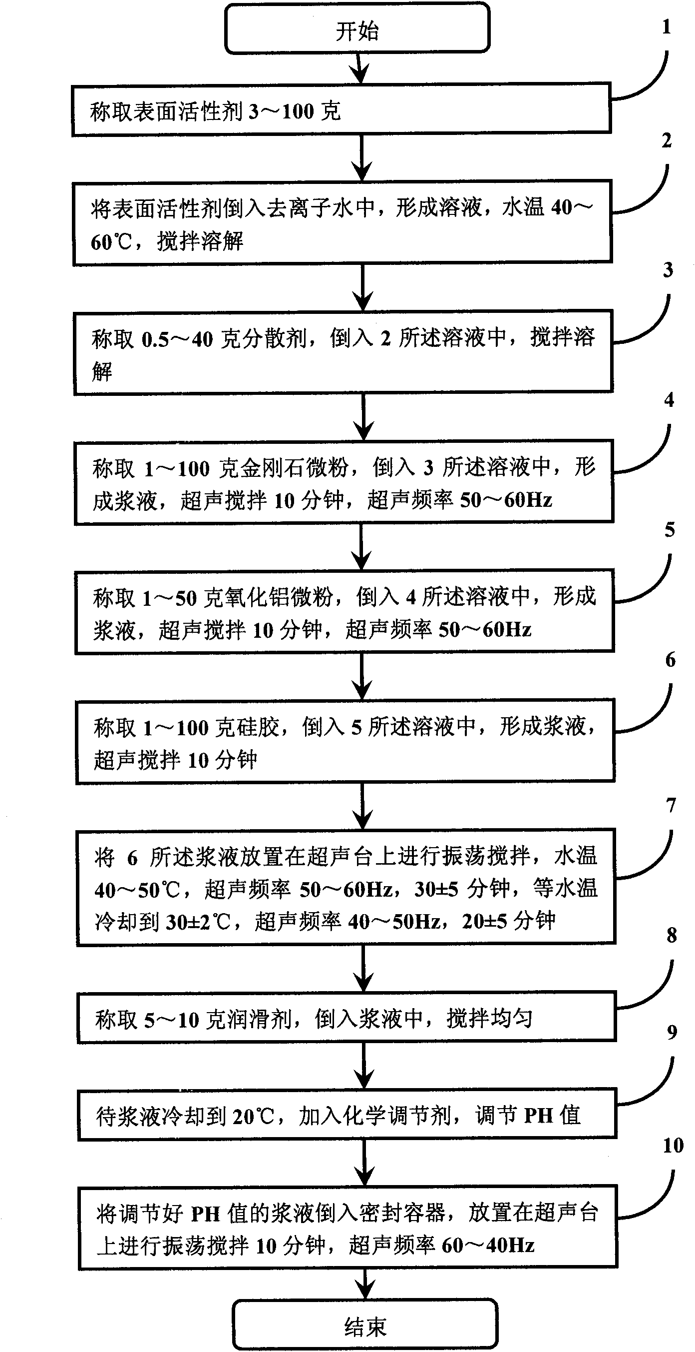
[0038] In order to make the object, technical solution and advantages of the present invention clearer, the present invention will be described in further detail below in conjunction with specific embodiments and with reference to the accompanying drawings.

[0039] When the thinning process enters the polishing stage, synthetic discs with soft texture and good elastic coefficient should be used, such as tin discs, antimony discs, resin discs, etc., and a matching polishing solution is required.

[0040] The nano-scale polishing liquid provided by the present invention adopts the following components: (1) diamond micropowder: particle size 30nm~500nm; (2) alumina micropowder: particle size 30nm~1μm; (3) silica gel (silicon oxide hydrate) : Particle size 30nm~1μm; (4) Surfactant: Sodium dodecylbenzenesulfonate / Sodium dodecyl sulfate / Maleic anhydride mixture; (5) Dispersant: Sodium silicate / Sodium hypochlorite / Sodium pyrophosphate mixture; (6) lubricant: polyethylene glycol; (7...


PUM

PropertyMeasurementUnit
diameteraaaaaaaaaa
diameteraaaaaaaaaa
particle diameteraaaaaaaaaa

Abstract

The invention discloses a nanometer level polishing solution and a preparation method thereof. The polishing solution is prepared from the following components in percentage by mass: 0.1 to 10 percent of monocrystal artificial diamond micro powder, 0.1 to 5 percent of aluminum oxide micro powder, 0.1 to 10 percent of silica gel, 0.3 to 10 percent of surfactant, 0.05 to 4 percent of dispersing agent, 0.5 to 1 percent of lubricant, 0.01 to 1 percent of chemical PH value regulator and 60 to 98.2 percent of solvent. The invention also discloses the preparation method for the nanometer level polishing solution. By the method, mixed serous fluid is prepared from the nanometer level diamond, the aluminum oxide and the silica gel, so an ideal polishing effect is achieved, the requirement of a process for thinning and grinding substrates (silicon carbide and sapphire) for GaN extension is met, and a technical means is provided for a polishing process for semiconductors.

Description

technical field [0001] The invention relates to the technical field of semiconductor processing, in particular to a nano-scale polishing liquid and a preparation method thereof. Background technique [0002] Gallium nitride (GaN), as the third-generation wide-bandgap semiconductor material, has a large bandgap (3.4eV), a high breakdown voltage (3.3MV / cm), and a high two-dimensional electron gas concentration (>10 13 cm 2 ), high velocity of saturated electrons (2.8×10 7 cm / s) and other characteristics have received extensive attention internationally. The application of GaN in devices is regarded as the most important event in semiconductors in the 1990s. At present, the high frequency, high voltage, high temperature and high power characteristics of AlGaN / GaN HEMT devices make them have great prospects in microwave power devices. At the same time, GaN has brought semiconductor light-emitting diodes and lasers to a new level. [0003] GaN is a direct bandgap semicondu...

Claims


Application Information

Patent Timeline
Patent Type & Authority Applications(China)
IPC IPC(8): C09G1/02
Inventor 汪宁陈晓娟罗卫军庞磊刘新宇
Owner INST OF MICROELECTRONICS CHINESE ACAD OF SCI
Why Eureka
Try Eureka