Poisonous and harmful gas detection chip and preparation method thereof
A technology for detecting harmful gases and chips, applied in measuring devices, material analysis through electromagnetic means, instruments, etc., can solve problems such as no substantive breakthroughs, achieve detection cost automation, small individual differences in chips, and flexible combination Effect
- Summary
- Abstract
- Description
- Claims
- Application Information
AI Technical Summary
Problems solved by technology
Method used
Image
Examples
Embodiment 1
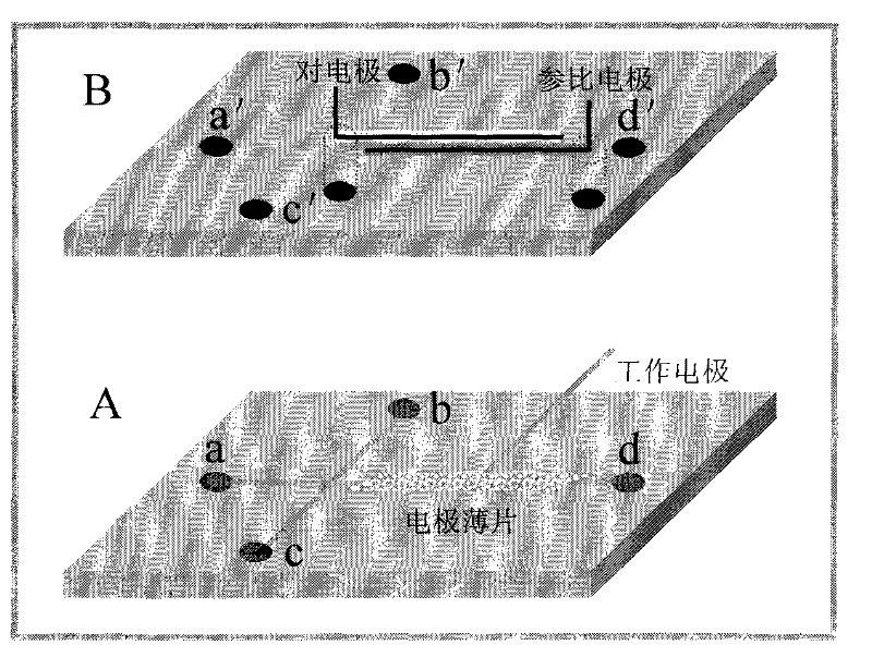
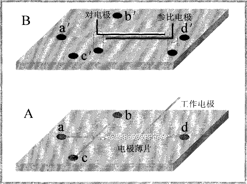
[0034]Use computer-aided design (CAD) to draw the microchannel pattern of the microfluidic chip, and then use the laser printer to print the pattern as a photomask, and then use an excimer laser etching machine to prepare on the surface of polymethyl methacrylate (PMMA) substrate. Chip microchannel network required. After cutting the PMMA substrate, wash it with ethanol, deionized water, and ethanol, and then dry it naturally to obtain two pieces of PMMA chips (5×5 cm) up and down. After calcining multi-walled carbon nanotubes (MWNTs) at 550 °C for 30 min, put them into concentrated mixed acid (concentrated nitric acid / concentrated perchloric acid, volume ratio 7:3) for ultrasonic oscillation for 30 min, boil and reflux for 2 h under magnetic stirring, and filter Rinse repeatedly with twice distilled water, then with ethanol, and dry at 80°C for later use. The Pt sheet (0.4×0.4mm) was repeatedly polished with fine metallographic sandpaper, and then corroded in newly prepared ...
Embodiment 2
[0036] Use computer-aided design (CAD) to draw the microchannel pattern of the microfluidic chip, and use soft etching technology (photolithography-mask) to etch the required microchannel network on the surface of the upper and lower glass (5×5cm) . Clean the glass chip base material with detergent, deionized water, ethanol, deionized water and ethanol, and then dry it naturally to obtain upper and lower PC chips (5×5 cm). The working electrode (Pt sheet, 0.4×0.4mm) was laser etched to obtain multiple ~1 micron lattices on the surface, and then electrochemical platinum deposition was performed. Nano-scale platinum particles were deposited on the surface of the platinum sheet to obtain a surface with micro / Nanostructured platinum electrodes. The counter electrode (platinum electrode) and reference electrode (silver chloride / silver electrode) were placed in the electrode microgrooves of the upper chip, and the working electrode (platinum electrode) was placed in the microgroov...
PUM
 Abstract
Description
Claims
Application Information

