Fabrication method for crystalline silicon solar cell

A solar cell and manufacturing method technology, applied in circuits, electrical components, semiconductor devices, etc., can solve problems such as cost increase, waste of phosphorus source, complicated process flow, etc. cost effect

Inactive Publication Date: 2012-01-25
NINGBO INST OF MATERIALS TECH & ENG CHINESE ACADEMY OF SCI
View PDF2 Cites 16 Cited by
  • Summary
  • Abstract
  • Description
  • Claims
  • Application Information

AI Technical Summary

Problems solved by technology

[0004] The above-mentioned conventional manufacturing process has the following disadvantages: (1) when one surface of the crystalline silicon wafer is formed by high-temperature diffusion doping to form a PN junction, parasitic diffusion usually occurs on the other side of the crystalline silicon wafer, thereby requiring a back junction removal process, resulting in The process is complicated; (2) thicker phosphosilicate glass will be formed during the PN junction diffusion process, which contains a large amount of phosphorus atoms, which need to be removed by highly polluted hydrofluoric acid solution, so on the one hand, it will lead to a lot of waste of phosphorus sources, On the other hand, due to the use of a large amount of highly polluted hydrofluoric acid solution, the process waste liquid needs to be treated, resulting in increased costs

Method used


Image

  • Fabrication method for crystalline silicon solar cell
  • Fabrication method for crystalline silicon solar cell
  • Fabrication method for crystalline silicon solar cell

Examples


Embodiment 1

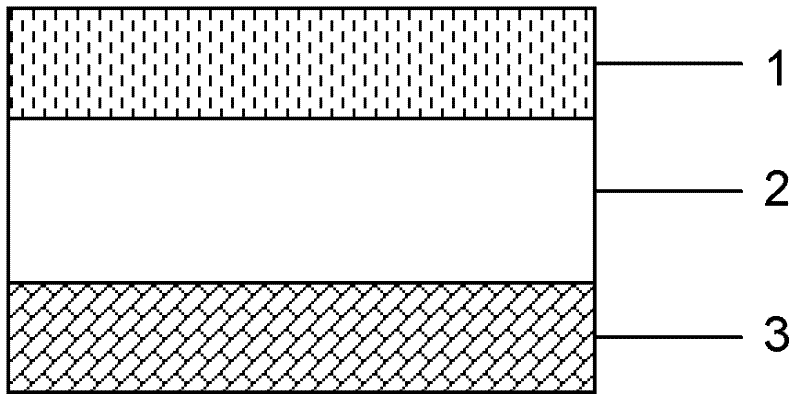
[0044] In this embodiment, the p-type crystalline silicon substrate 2 adopts a p-type single crystal silicon wafer, and the boron-containing silicon nitride film or boron nitride film 3 adopts a boron-containing silicon nitride film, which is obtained by the manufacturing method of the present invention A cutaway view of a crystalline silicon solar cell image 3 As shown, the specific production process is as follows:

[0045] Step 1: cleaning the p-type crystalline silicon substrate 2 with a conventional cleaning method, and using an alkaline solution to make a suede surface;

[0046] Step 2: Put the p-type crystalline silicon substrate 2 in the PECVD reaction chamber, pass through silane, ammonia gas and a small amount of phosphine, and deposit phosphorus on the front surface of the p-type crystalline silicon substrate 2 at a reaction temperature of 300°C silicon nitride film 1, the thickness of the phosphorus-containing silicon nitride film 1 is 70nm;

[0047] Step 3: Tak...

Embodiment 2

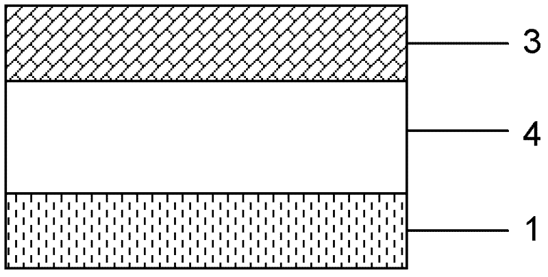
[0053] In this embodiment, the p-type crystalline silicon substrate 2 adopts a p-type single crystal silicon wafer, the boron-containing silicon nitride film or boron nitride film 3 adopts a boron nitride film, and the crystalline silicon solar energy obtained by the manufacturing method of the present invention The three-dimensional cutaway view of the battery is similar to image 3 As shown, the specific production process is as follows:

[0054] The concrete manufacturing method of crystalline silicon solar cell comprises the following steps:

[0055] Step 1: cleaning the p-type crystalline silicon substrate 2 with a conventional cleaning method, and using an alkaline solution to make a suede surface;

[0056] Step 2: Put the p-type crystalline silicon substrate 2 in the PECVD reaction chamber, pass through silane, ammonia gas and a small amount of phosphine, and deposit phosphorus on the front surface of the p-type crystalline silicon substrate 2 at a reaction temperature...

Embodiment 3

[0063] In this embodiment, the p-type crystalline silicon substrate 2 adopts a p-type single crystal silicon wafer, the boron-containing silicon nitride film or boron nitride film 3 adopts a boron nitride film, and the crystalline silicon solar energy obtained by the manufacturing method of the present invention The three-dimensional cutaway view of the battery is shown in image 3 As shown, the specific production process is as follows:

[0064] Step 1: cleaning the p-type crystalline silicon substrate 2 with a conventional cleaning method, and using an alkaline solution to make a suede surface;

[0065] Step 2: Put the p-type crystalline silicon substrate 2 in the PECVD reaction chamber, pass through silane, ammonia gas and a small amount of phosphine, and deposit phosphorus on the front surface of the p-type crystalline silicon substrate 2 at a reaction temperature of 350°C silicon nitride film 1, the thickness of the phosphorus-containing silicon nitride film 1 is 70nm; ...


PUM

PropertyMeasurementUnit
thicknessaaaaaaaaaa
thicknessaaaaaaaaaa

Abstract

The invention discloses a fabrication method for a crystalline silicon solar cell. A phosphorous silicon nitride film is deposited on one surface of a P-type crystalline silicon wafer or an N-type crystalline silicon wafer after cleaning and etching, a boron nitride film or a boracic silicon nitride film is deposited on the other surface, the crystalline silicon wafer with deposited films is then annealed under high temperature, so that the elements of phosphorus and boron in the films can be diffused into the crystalline silicon wafer, consequently, the P-type crystalline silicon wafer is formed into a N plus PP plus structure, the N-type crystalline silicon wafer is formed into a P plus NN plus structure, afterwards, metal electrodes are fabricated, and the fabrication of the cell is fulfilled. Compared with the conventional fabrication method, the fabrication method integrates the high-temperature diffusion doping process for forming the PN junction and the preparation process of an antireflection film together, avoids the edge junction etching process, and reduces the usage of phosphorus source and boron source, thus greatly simplifying the process flow and reducing the fabrication cost, and the fabrication method has a broad application prospect in the technical field of solar cell fabrication.

Description

technical field [0001] The invention relates to the technical field of crystalline silicon solar cells, in particular to a method for manufacturing a crystalline silicon solar cell. Background technique [0002] As one of the important ways of solar energy application, solar cells have attracted widespread attention from all over the world. After years of development, a variety of solar cell materials have been researched and developed. Among them, crystalline silicon solar cells occupy more than 80% of the photovoltaic market due to their high photoelectric conversion efficiency, mature technology and sufficient raw materials. [0003] At present, the production process of crystalline silicon solar cells mainly includes: (1) cleaning and texturing treatment, that is, cleaning and removing the damaged layer on the surface of crystalline silicon wafers, and then performing alkali etching on the surface of single crystal silicon wafers or acid etching on the surface of polycr...

Claims


Application Information

Patent Timeline
Patent Type & Authority Applications(China)
IPC IPC(8): H01L31/18
CPCY02P70/50
Inventor 万青竺立强张洪亮
Owner NINGBO INST OF MATERIALS TECH & ENG CHINESE ACADEMY OF SCI
Why Eureka
Try Eureka