Chip transporting system of plasma etcher for carrying out dry etching on inorganic material substrate

An inorganic material and plasma technology, applied in the field of film transfer systems, can solve the problems of poor reliability and low transfer efficiency, and achieve the effects of good reliability, high transfer efficiency, and simple and reasonable structure.

Inactive Publication Date: 2012-03-07
JIAXING KEMIN ELECTRONICS EQUIP TECH
View PDF4 Cites 2 Cited by
  • Summary
  • Abstract
  • Description
  • Claims
  • Application Information

AI Technical Summary

Problems solved by technology

[0009] The present invention solves the problems of low film transfer efficiency and poor reliability in the existing ICP etching machine film transfer system,

Method used


Image

  • Chip transporting system of plasma etcher for carrying out dry etching on inorganic material substrate
  • Chip transporting system of plasma etcher for carrying out dry etching on inorganic material substrate
  • Chip transporting system of plasma etcher for carrying out dry etching on inorganic material substrate

Examples


Embodiment Construction

[0032] The present invention will be further described below in conjunction with specific examples, but the present invention is not limited to these specific implementations. Those skilled in the art will realize that the present invention covers all alternatives, modifications and equivalents as may be included within the scope of the claims.

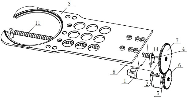
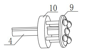
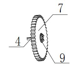
[0033] refer to Figure 1-4 , a film transfer system of a plasma etching machine for dry etching inorganic material substrates, which is installed in a pre-vacuum chamber 12 and includes a manipulator 3 for transporting a disc, and the manipulator 3 is fixedly connected to a screw rod that drives its movement On nut 8, described screw mandrel nut 8 is installed on the screw mandrel 11, and described screw mandrel 11 is connected with servo motor 1 by gear pair, and described gear pair comprises main gear 6 that is connected with servo motor rotor 5, and screw mandrel The rotor 4 is connected to the pinion gear 7 , and the main gear 6...


PUM


Abstract

The invention relates to a chip transporting system of a plasma etcher for carrying out dry etching on an inorganic material substrate, which is arranged in a forevacuum cavity and comprises a manipulator for transporting a chip dish. The manipulator is fixedly connected onto a screw nut for driving the manipulator to move. The screw nut is arranged on a screw. The screw is connected with a servo motor through a gear pair. The gear pair comprises a main gear connected with a rotor of the servo motor and a pinion connected with a rotor of the screw. The main gear is in meshed connection with the pinion. The chip transporting system has the beneficial effects of high chip transporting efficiency, high reliability and simple and reasonable structure.

Description

technical field [0001] The invention relates to a film transfer system of a dry etching inorganic material substrate plasma etching machine. Background technique [0002] Etching is a very important process step in semiconductor manufacturing process, microelectronic IC manufacturing process and micro-nano manufacturing process, and is a main process of patterning (pattern) processing associated with lithography. The so-called etching, in fact, is understood in a narrow sense as photolithography etching. First, the photoresist is subjected to photolithography exposure treatment by photolithography, and then the part to be removed is etched by other means. With the development of micro-manufacturing technology, in a broad sense, etching has become a general term for stripping and removing materials through solutions, reactive ions or other mechanical methods, and has become a common name for micro-machining. The simplest and most commonly used classifications of etching are ...

Claims


Application Information

Patent Timeline
IPC IPC(8): H01L21/67H01J37/02H01J37/32B25J9/08
Inventor 李超波黄成强陈波饶志鹏
Owner JIAXING KEMIN ELECTRONICS EQUIP TECH
Why Eureka
Try Eureka