Interface treatment technology for hetero junction solar cell

A solar cell and silicon heterojunction technology, which is applied in the field of preparation of heterojunction solar cells, can solve the problems of effective antireflection and surface passivation of difficult-to-high-efficiency cells, difficult to control the thickness of the oxide layer, and difficult industrialization process, etc. Achieve the effect of improving the performance of the heterojunction interface, improving the conversion efficiency, and strong operability

Inactive Publication Date: 2012-03-21
CHANGZHOU HETE PHOTOELECTRIC
View PDF5 Cites 14 Cited by
  • Summary
  • Abstract
  • Description
  • Claims
  • Application Information

AI Technical Summary

Problems solved by technology

Among them, the deposition of doped silicon film on the surface is mainly realized by PECVD technology, which has high requirements for PECVD process, and the high doping concentration will cause the decrease of open circuit voltage; the preparation of oxide layer on the surface of crystalline silicon by thermal oxidation method can be better Passivate the surface, but the thickness of the ultra-thin oxide layer is difficult to control, and the industrialization process is difficult. What's more, due to the low refractive index of silicon dioxide, it is difficult to meet the dual functions of effective anti-reflection and surface passivation of high-efficiency batteries at the same time

Method used


Image

  • Interface treatment technology for hetero junction solar cell

Examples


Embodiment Construction

[0038] In order to make the technical scheme and advantages of the present invention clearer, the invention is further described in detail in conjunction with specific examples:

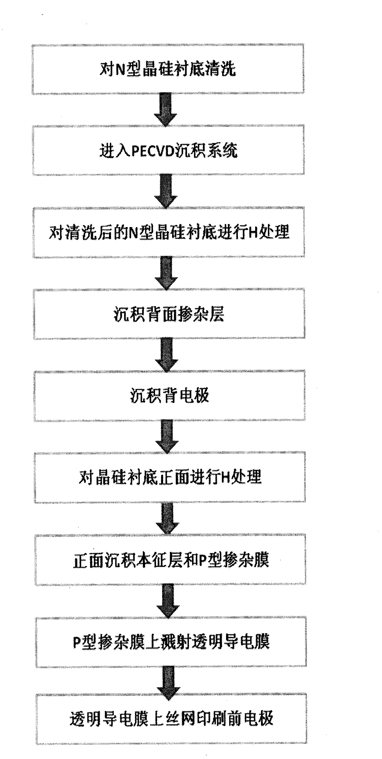
[0039] 1) An N-type monocrystalline silicon wafer with a thickness of 200 μm and a resistivity of 5 Ωcm is used as a substrate, and the surface is routinely cleaned.

[0040] 2) Send the cleaned N-type crystalline silicon substrate into the PECVD system, and make the reaction gas H 2 Ionization produces H;

[0041] 3) Treat the silicon surface with H at low temperature (<250°C) for 40s;

[0042] 4) Deposit a layer of heavily doped a-Si with a thickness of 20nm: a passivation layer made of H on the processed N-type single crystal silicon wafer substrate;

[0043] 5) Depositing a ZnO:B conductive film on the surface of the passivation layer by MOCVD method as the back electrode;

[0044] 6) As described in 2) and 3), carry out H treatment to the front side of the N-type monocrystalline silicon wafer...


PUM

PropertyMeasurementUnit
thicknessaaaaaaaaaa
thicknessaaaaaaaaaa

Abstract

The invention discloses an interface treatment technology for a hetero junction solar cell. The method is characterized in that: the technology can be applied to the manufacturing of a thin film/crystalline silicon hetero junction solar cell, reaction gases can be ionized by utilizing a plasma enhanced chemical vapor deposition (PECVD) system or a hotwire chemical vapor deposition (HWCVD) system to generate H, and the H is transported to a crystalline silicon substrate by a gas phase and reacted with the surface of crystalline silicon to effectively passivate defect states such as unsaturated dangling bonds and the like on the surface of the crystalline silicon, reduce hetero junction interface recombination and facilitate improvement in the overall performance of the hetero junction solar cell.

Description

technical field [0001] The invention relates to the preparation of heterojunction solar cells, in particular to an interface treatment method for improving the performance of heterojunction solar cells. technical background [0002] Heterojunction solar cells deposit P-type (N-type) silicon films on N-type (P-type) crystalline silicon wafers as emitters, and form heterojunction structures at the interface between the film and crystalline silicon. The junction performance plays a decisive role. Usually, there are a large number of unsaturated dangling bonds and other defect states on the surface of crystalline silicon, which increases the recombination of the heterojunction interface, seriously affects the open circuit voltage of the cell, and limits the conversion efficiency of the solar cell. It can be seen that, Crystal-silicon interface treatment plays a vital role in improving the efficiency of heterojunction solar cells and improving the stability of the cells. [0003...

Claims


Application Information

Patent Timeline
Patent Type & Authority Applications(China)
IPC IPC(8): H01L31/18C23C16/455H01L31/04H01L31/068H01L31/077
CPCY02E10/50Y02E10/547Y02P70/50
Inventor 张群芳
Owner CHANGZHOU HETE PHOTOELECTRIC
Why Eureka
Try Eureka