Methods for preparing and performing photocurrent testing on CoPc/TiO2 composite semiconductor nano material

A compound semiconductor and nano-material technology, applied in the field of photoelectric conversion, can solve the problems of low quantum efficiency, short lifetime of photogenerated electrons and holes, etc., and achieve the effects of high charge transfer efficiency, convenient electron transfer, and good stability

Inactive Publication Date: 2012-04-04
NORTHWEST NORMAL UNIVERSITY
View PDF1 Cites 3 Cited by
  • Summary
  • Abstract
  • Description
  • Claims
  • Application Information

AI Technical Summary

Problems solved by technology

[0002] TiO 2 is a wide bandgap semiconductor (E g =3.2eV), as a photocatalyst has been highly valued, TiO 2 It mainly absorbs ultraviolet light with a wavelength of less than 350nm. However, ultraviolet light only accounts for 5% of natural light. In addition, there are shortcomings such as short lifetime of photogenerated electron-hole pairs and low quantum efficiency of photocatalytic process.

Method used


Image

  • Methods for preparing and performing photocurrent testing on CoPc/TiO2 composite semiconductor nano material
  • Methods for preparing and performing photocurrent testing on CoPc/TiO2 composite semiconductor nano material
  • Methods for preparing and performing photocurrent testing on CoPc/TiO2 composite semiconductor nano material

Examples


Embodiment Construction

[0041] In conjunction with accompanying drawing, technical scheme of the present invention is described further:

[0042] 1. Instruments and reagents used in this experiment

[0043] The water used in the experiment process is double-distilled water, and the reagents used in the experiment are all analytically pure. The instruments and reagents used in this experiment: visible light source LA-410UV-3 (Japan HAYASHI Instrument Company), CHI900 (US CH Instrument Company) ) for scanning E-t, I-t curves, Ag / AgCl reference electrode (CHI111, US CH Instrument Company), platinum counter electrode, quartz tube heating automatic double pure water still (1810B, Shanghai Asia-Pacific Technology Glass Company) for distilling Secondary distilled water, electronic balance (Beijing Sartorius Instrument Co., Ltd.) for weighing medicines, ML-902 magnetic stirrer (Shanghai Pujiang Analytical Instrument Factory) to stir and synthesize nano-semiconductor materials, FURWACE (Tianjin Zhonghuan Expe...


PUM


Abstract

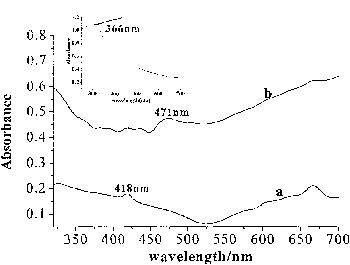
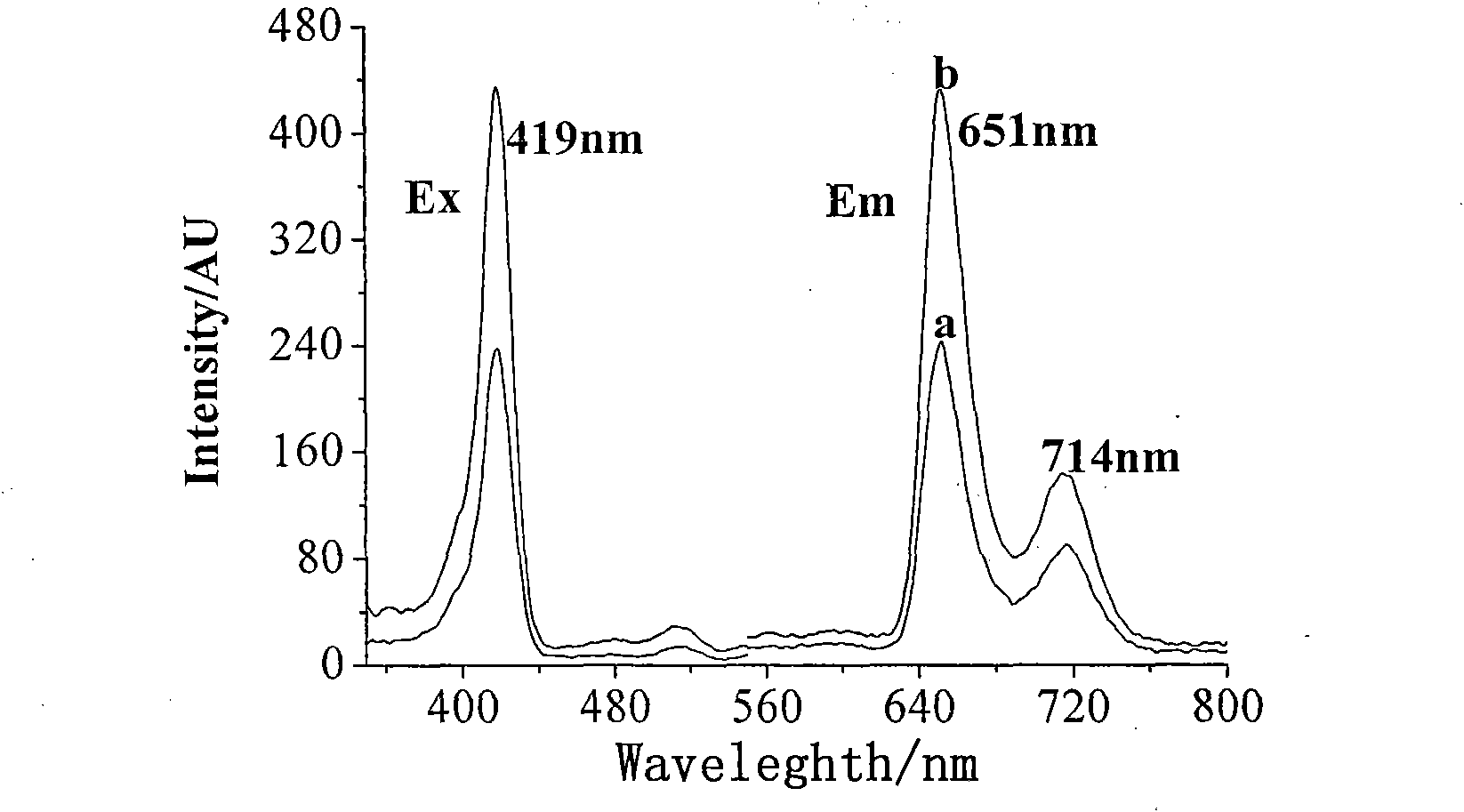
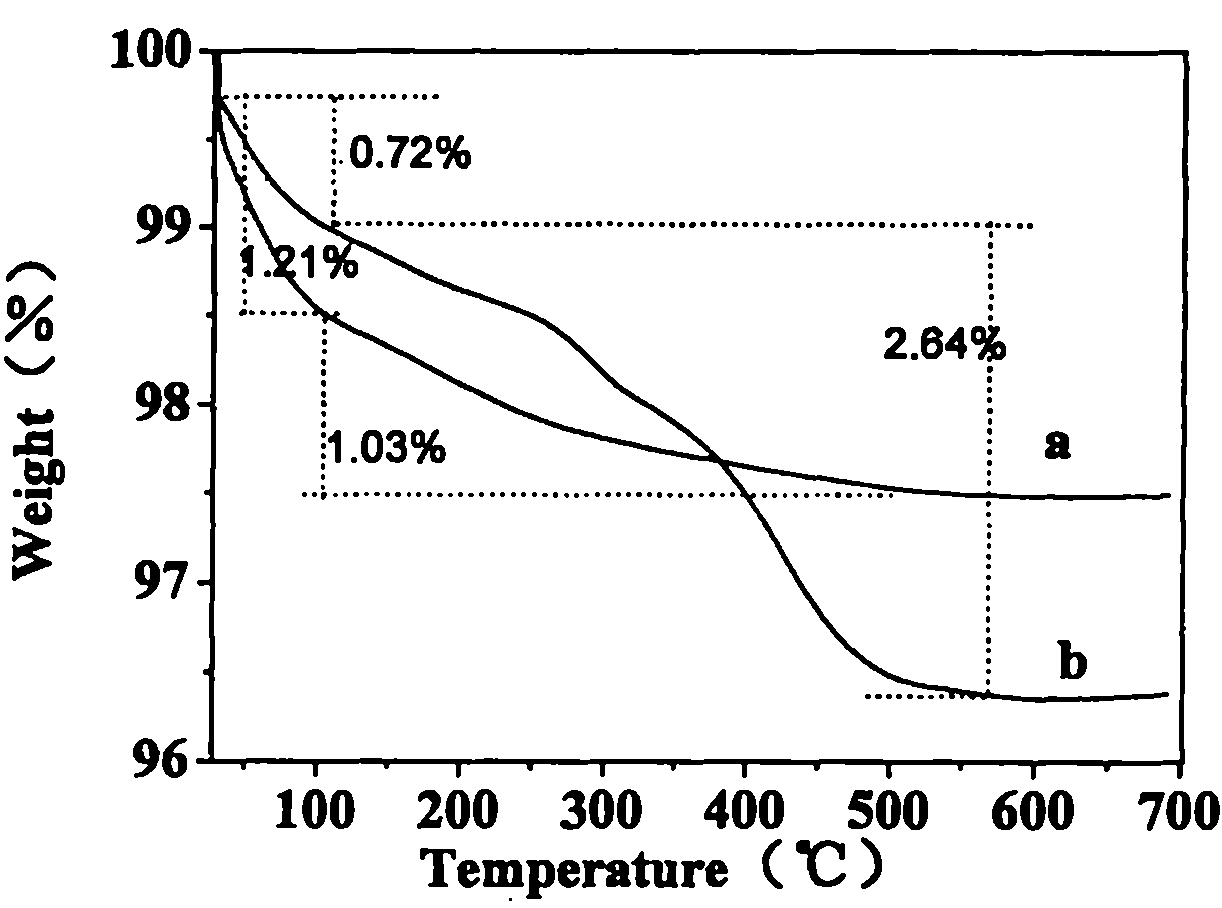
The invention relates to a composite semiconductor nano material which is prepared by calcining nano titanium dioxide (TiO2) and cobalt phthalocyanine (CoPc) as the raw materials at a temperature of below 500 DEG C. By means of an ultraviolet-visible absorption spectrum, a fluorescence spectrum, thermogravimetric analysis and the like, the CoPc / TiO2 composite semiconductor nano material is characterized, and the photoelectrochemical properties, i.e. an open circuit potential-time (Eoc-t) and a relation (I-t) that a current changes with time, of the composite semiconductor nano material are measured. A result shows that under the condition of visible light induction, when an electrondonating substance, i.e. hydroquinone (HQ), is added, electron transfer can occur and a photocurrent can be generated after a circuit is switched on.

Description

technical field [0001] The present invention relates to a kind of CoPc / TiO 2 Preparation of compound semiconductor nanomaterials and photoelectric conversion of materials. The CoPc / TiO 2 Characterization of compound semiconductor nanomaterials and measurement of photoelectrochemical properties of compound semiconductor nanomaterials〔E oc -t, I-t]. Background technique [0002] TiO 2 is a wide bandgap semiconductor (E g =3.2eV), as a photocatalyst has been highly valued, TiO 2 It mainly absorbs ultraviolet light with a wavelength of less than 350nm, but ultraviolet light only accounts for 5% of natural light. In addition, it also has the disadvantages of short lifetime of photogenerated electron-hole pairs and low quantum efficiency of photocatalytic process. For this reason, researchers mainly focus on methods such as doping or surface modification to broaden the TiO 2 Light wavelength response range to improve photocatalytic quantum efficiency. Phthalocyanine is a m...

Claims


Application Information

Patent Timeline
IPC IPC(8): B82B3/00G01R19/00
Inventor 卢小泉张翠忠仵博万赵东霞王金凤张霞李莉乔志刚
Owner NORTHWEST NORMAL UNIVERSITY
Why Eureka
Try Eureka