

Preparation method and structure of one-film and multipurpose masked texturing solar cell
A solar cell and mask technology, which is applied in circuits, photovoltaic power generation, electrical components, etc., can solve the problems of large equipment investment and high equipment requirements, and achieve the effects of simple process, low cost, and high photoelectric conversion efficiency
- Summary
- Abstract
- Description
- Claims
- Application Information
AI Technical Summary
Problems solved by technology
Method used
Image


Examples
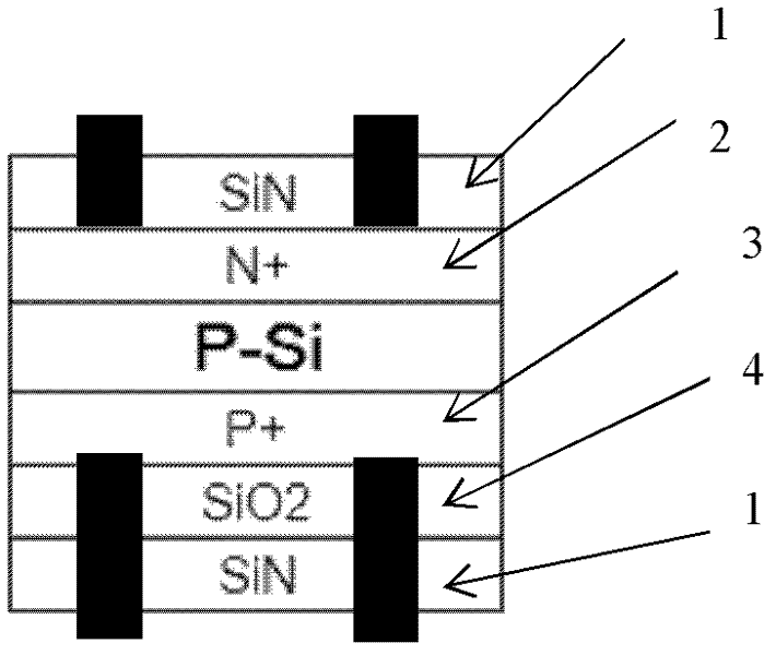
Embodiment 1
[0047] Select P-type Czochralski monocrystalline silicon chip, crystal direction (100), doping concentration 1Ωcm as example, the present invention is further described, has the following steps:
[0048] a) Both sides of the silicon wafer are polished;
[0049] b) BBr3 liquid boron diffusion source is used to prepare P-type backside field, the diffusion temperature is 930°C, the time is 50min, and the sheet resistance is 30ohm / Sq;
[0050] c) Etch the P-type emitter junction on the back and remove the BSG at the same time with the post-cleaning machine of RENA company;
[0051] d) growing a SiO2 thin film by thermal oxidation as a mask layer with a thickness of 300nm;
[0052] e) re-depositing a 90nm SiNx film on the back;
[0053] f) etching the SiO2 film on the non-emitter surface with a corrosive slurry;
[0054] g) use conventional alkali texturing solution to make texturing on the front side, and SiO2 film / SiNx film as the mask on the back;
[0055] h) The P-N junctio...
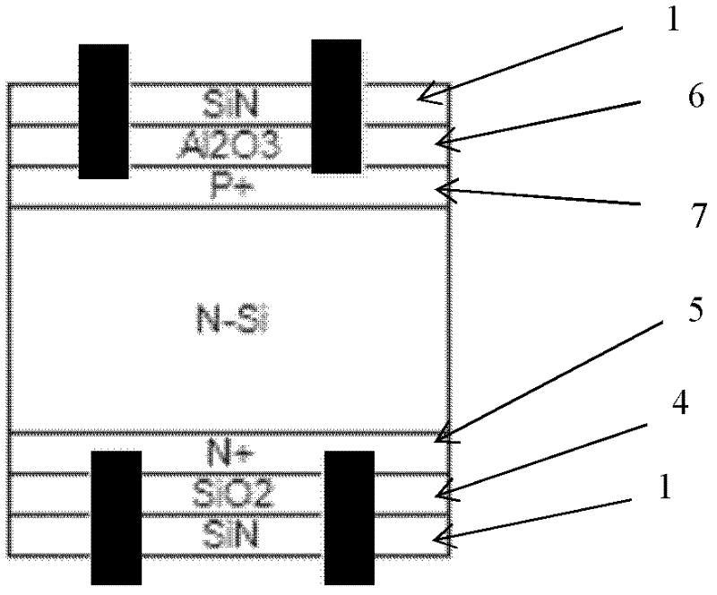
Embodiment 2
[0067] Select n-type Czochralski monocrystalline silicon chip, crystal direction (100), doping concentration 1Ωcm as example, the present invention is further described, has the following steps:
[0068] a) Both sides of the silicon wafer are polished;
[0069] b) N-type back field was prepared by POCl3 liquid phosphorus diffusion source, the diffusion temperature was 850°C, the time was 50min, and the sheet resistance was 30ohm / Sq;
[0070] c) Etch the N-type back field on the back and remove the PSG at the same time with the post-cleaning machine of RENA company;
[0071] d) growing a SiO2 thin film mask layer with a thickness of 300nm by thermal oxidation;
[0072] e) re-depositing a 90nm SiN film on the back;
[0073] f) etching the SiO2 mask layer on the non-emitter surface with a corrosive slurry;
[0074] g) use conventional alkali texturing solution to make texturing on the front side, and use SiO2 / SiNx as the mask on the back side;
[0075] h) BBr3 liquid boron di...
PUM
| Property | Measurement | Unit |
|---|---|---|
| thickness | aaaaa | aaaaa |
| thickness | aaaaa | aaaaa |
| refractive index | aaaaa | aaaaa |
Abstract
Description
Claims
Application Information