Growing method for low-dislocation gallium nitride
A growth method, gallium nitride technology, applied in the field of semiconductor material growth, can solve problems that affect the quality of material crystals and limit the photoelectric performance of devices
- Summary
- Abstract
- Description
- Claims
- Application Information
AI Technical Summary
Problems solved by technology
Method used
Image

Examples
Embodiment Construction
[0025] see Figure 1 to Figure 4 As shown, the present invention provides a method for growing low dislocation gallium nitride, comprising the following steps:
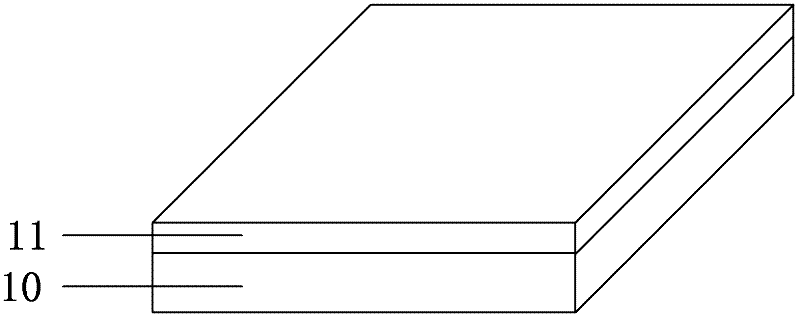
[0026] Step 1: get a substrate, which includes a substrate 10 and a gallium nitride template 11 made thereon (see figure 1 ), the substrate here can be sapphire, SiC, Si, GaAS, GaN, and the epitaxial material on the substrate can be InP, GaAs, GaN, AlN, InN, InGaN, AlGaN, AlInN, AlInGaN and other ternary and quaternary III- Group V and IV-VI compound semiconductors.
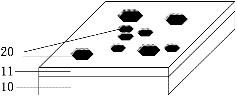
[0027] Step 2: corrode the surface of the gallium nitride template 11 with an etching solution, and form a hexagonal micropit 20 on the surface of the gallium nitride template 11 (see figure 2 ), the corrosion solution is KOH solution, the temperature is 80°C, the corrosion time is 1-2min, or the volume ratio of the corrosion solution is H 2 SO 4 :H 3 PO 4 = 3:1, the temperature is 260°C, the etching time is 4-8min, the depth of the hexagonal micr...
PUM
 Abstract
Description
Claims
Application Information
 - R&D Engineer
- R&D Manager
- IP Professional
- Industry Leading Data Capabilities
- Powerful AI technology
- Patent DNA Extraction
Browse by: Latest US Patents, China's latest patents, Technical Efficacy Thesaurus, Application Domain, Technology Topic.
© 2024 PatSnap. All rights reserved.Legal|Privacy policy|Modern Slavery Act Transparency Statement|Sitemap