Packaging structure of OLED

A technology of electroluminescent devices and packaging structures, which is applied in the direction of electric solid devices, electrical components, semiconductor devices, etc., can solve the problems of device film structure defects, difficult to realize flexible coil production, complex processing technology, etc., and achieve equipment saving Investment cost and floor area, blocking the penetration of water and oxygen into the device, and the effect of low deposition temperature

Inactive Publication Date: 2012-05-02
SICHUAN CHANGHONG ELECTRIC CO LTD
View PDF3 Cites 24 Cited by
  • Summary
  • Abstract
  • Description
  • Claims
  • Application Information

AI Technical Summary

Problems solved by technology

2. The carbonyl compound produced by the oxidation of oxygen and the light-emitting layer is an effective quencher, which will significantly reduce the luminous quantum efficiency of organic electroluminescent devices
Water vapor hydrolyzes the organic layer compound and affects the conductivity, resulting in greatly reduced stability
3. The heat generated when the organic electroluminescent device is working will further aggravate the aging of the luminescent materials, auxiliary materials, electrodes, etc. in the organic electroluminescent device in the air, thereby affecting the service life of the device
Compared with glass substrates, plasti

Method used


Image

  • Packaging structure of OLED
  • Packaging structure of OLED
  • Packaging structure of OLED

Examples


Embodiment 1

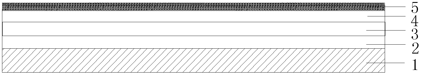
[0025] Such as figure 1 The packaging structure of the organic electroluminescent device shown in the present invention includes a substrate 1 of an electroluminescent device made of glass, and an anode 2, an organic layer 3 and a cathode 4 of the organic electroluminescent device are arranged on one side of the substrate 1. An encapsulation layer 5 is provided on the outside of the cathode 4, and the encapsulation layer 5 is a multi-layer composite film structure in which at least two inorganic insulating materials are alternately deposited by an atomic layer deposition system.

[0026] Such as figure 2 As shown, after the unpackaged organic electroluminescent device is placed in the atomic layer deposition system, the mask plate is aligned to cover the device lead-out electrode, and a high-purity inert gas is introduced. After vacuuming, the cathode of the light-emitting device 4. Deposit Al with a thickness of 2-5nm on the 2 o 3 film layer, and then in the Al 2 o 3 Th...

Embodiment 2

[0028] Such as image 3 As shown, on the basis of Example 1, the difference is to deposit Al with a thickness of 2-5 nm on the cathode 4 of the light-emitting device. 2 o 3 film layer, and then in the Al 2 o 3 The outer layer of the film layer is deposited with a thickness of 2-5nm Si 3 N 4 film layer, repeat the above film deposition steps 20 times (i.e. 20 layers), to obtain an Al with a thickness of 80-200nm 2 o 3 / Si 3 N 4 Membrane encapsulation layer 5.

Embodiment 3

[0030] On the basis of Embodiment 1 or 2, the substrate 1 is made of plastic, and packaging layers 5 are respectively provided on the outside of the cathode 4 and the inside of the substrate 1 .


PUM

PropertyMeasurementUnit
Thicknessaaaaaaaaaa
Thicknessaaaaaaaaaa
Thicknessaaaaaaaaaa

Abstract

The invention relates to a packaging structure of an OLED. The structure comprises a substrate of the OLED. One side of the substrate is provided with an anode of the OLED, an organic layer and a cathode. The outboard of the cathode is at least provided with a packaging layer. The packaging layer is a multilayer composite membrane structure which is formed by alternative deposition of two inorganic insulating materials through an atomic layer deposition system. The packaging structure of the OLED in the invention has a low deposition temperature. The organic layer of a luminescent device can not be damaged. Other organic film formation equipment is not needed. Equipment investment costs and land occupation areas can be saved. The inorganic film layer structure alternatively prepared by using an atomic layer deposition method is compact. Pinholes are less. Water and oxygen can be effectively avoided to penetrate into a device. A protection layer is processed on the packaging layer so as to effectively protect the packaging layer and obstruct the water and the oxygen.

Description

technical field [0001] The invention relates to an encapsulation structure of an organic electroluminescent device (OLED). Background technique [0002] Organic electroluminescent devices (OLEDs) have the characteristics of low power consumption, light weight, high brightness, wide field of view, high contrast and fast response, and can realize flexible displays well. Over the past ten years, organic electroluminescent devices have made great progress. Samsung, LG, Sony and other manufacturers have launched related application products, and other display manufacturers have also invested in research and development. [0003] At present, there are still some problems in the development of organic electroluminescent device technology. The short life of the device has largely restricted the process of industrialization of organic electroluminescent devices. The lifetime of an organic electroluminescent device is related to the performance and lifetime of the selected organic ma...

Claims


Application Information

Patent Timeline
IPC IPC(8): H01L51/50H01L51/52
CPCH10K50/8445
Inventor 彭德权潘晓勇李斌
Owner SICHUAN CHANGHONG ELECTRIC CO LTD
Why Eureka
Try Eureka