Integration method of dual Damascus

An integrated method and low dielectric constant technology, applied in the direction of electrical components, semiconductor/solid-state device manufacturing, circuits, etc., can solve the problems such as difficulty in controlling the key dimensions of through holes, affecting the reliability of copper interconnection, and connecting together, etc., to achieve Suitable for popularization and application, improving performance and reliability, and avoiding the effect of leakage current

Inactive Publication Date: 2012-05-09
SHANGHAI HUALI MICROELECTRONICS CORP
View PDF3 Cites 5 Cited by
  • Summary
  • Abstract
  • Description
  • Claims
  • Application Information

AI Technical Summary

Problems solved by technology

[0004] However, in these methods in the prior art, it is difficult to control the critical dimension of the through hole, and because the distance between the through hole and the through hole is small, it is easy to cause a large leakage current between the through hole and the through hole. What's more, it may also happ

Method used


Image

  • Integration method of dual Damascus
  • Integration method of dual Damascus
  • Integration method of dual Damascus

Examples


Embodiment Construction

[0029] The contact hole forming method for reducing the contact hole resistance of the present invention will be further described in detail below in conjunction with the accompanying drawings and specific implementation methods.

[0030] Such as figure 1 and Figure 2A-2I Shown, the integrated method of a kind of double damascene of the present invention, it comprises the following steps:

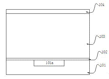
[0031] Step S1: Provide a silicon substrate 101, on which the completed front layer metal 101a is formed, and respectively adopt the chemical vapor deposition method to sequentially deposit via-hole etching barrier layers on the silicon substrate 101 from bottom to top 102, a low dielectric constant dielectric layer 103 and a dielectric protection layer 104;

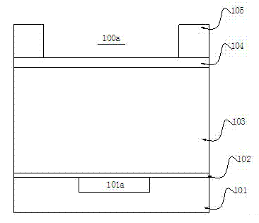
[0032] Step S2: Coating a layer of photoresist 105 on the dielectric protective layer 104 by spin coating, and performing a photolithography process (including exposure, development and other process steps) to form a trench opening...


PUM


Abstract

The invention discloses an integration method of dual Damascus, and the integration method uses a Damascus manufacturing process of digging trenches before vias. The method comprises the following steps: firstly depositing a metal hard mask when the vias are formed, thus effectively avoiding generating drain current and interlinkage between adjacent vias; reducing control difficulty of key sizes of the vias in an advanced copper process, improving the performance and reliability of a semiconductor device; and the technical process is simple and easy to control, and the method is suitable for popularizing application.

Description

technical field [0001] The invention relates to the technical field of semiconductor preparation, in particular to a double damascene integration method. Background technique [0002] In the production process of semiconductors, the miniaturization of semiconductor devices is also facing challenges due to the continuous increase in the integration of devices including, for example, MOSFETS (Metal Oxide Semiconductor Field Effect Transistors) and manufactured by means of MOS or CMOS processes. Not only the size and area of ​​the device needs to be reduced in size, but there are still high expectations in terms of quality and yield. The junction depth of this type of device involves high doping activity, good control of the junction depth, and so on. [0003] The so-called double damascene process is a common technique for opening via holes and trenches on the dielectric layer and filling them with metal and other materials. If the double damascene structure is classified ac...

Claims


Application Information

Patent Timeline
IPC IPC(8): H01L21/768
Inventor 姬峰陈玉文李磊胡友存张亮
Owner SHANGHAI HUALI MICROELECTRONICS CORP
Why Eureka
Try Eureka