Multi-piece multi-source horizontal hydride vapor phase epitaxy growth system

A hydride gas phase and epitaxial growth technology, which is applied in the growth of polycrystalline materials, single crystal growth, crystal growth, etc., can solve the problems that cannot meet the growth requirements of large quantities of GaN-based thick film materials

Active Publication Date: 2012-05-23
NANJING UNIV
View PDF7 Cites 6 Cited by
  • Summary
  • Abstract
  • Description
  • Claims
  • Application Information

AI Technical Summary

Problems solved by technology

[0005] The problem to be solved by the present invention is that the existing HVPE system cannot meet the growth requirements of large quantities of GaN-based thick film materials due to the limitations of internal structure and gas flow transportation.

Method used


Image

  • Multi-piece multi-source horizontal hydride vapor phase epitaxy growth system
  • Multi-piece multi-source horizontal hydride vapor phase epitaxy growth system
  • Multi-piece multi-source horizontal hydride vapor phase epitaxy growth system

Examples


Embodiment Construction

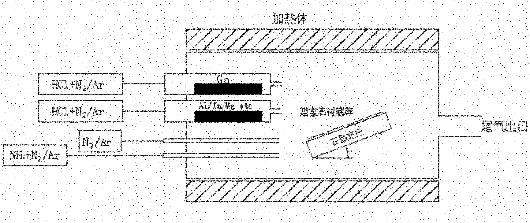
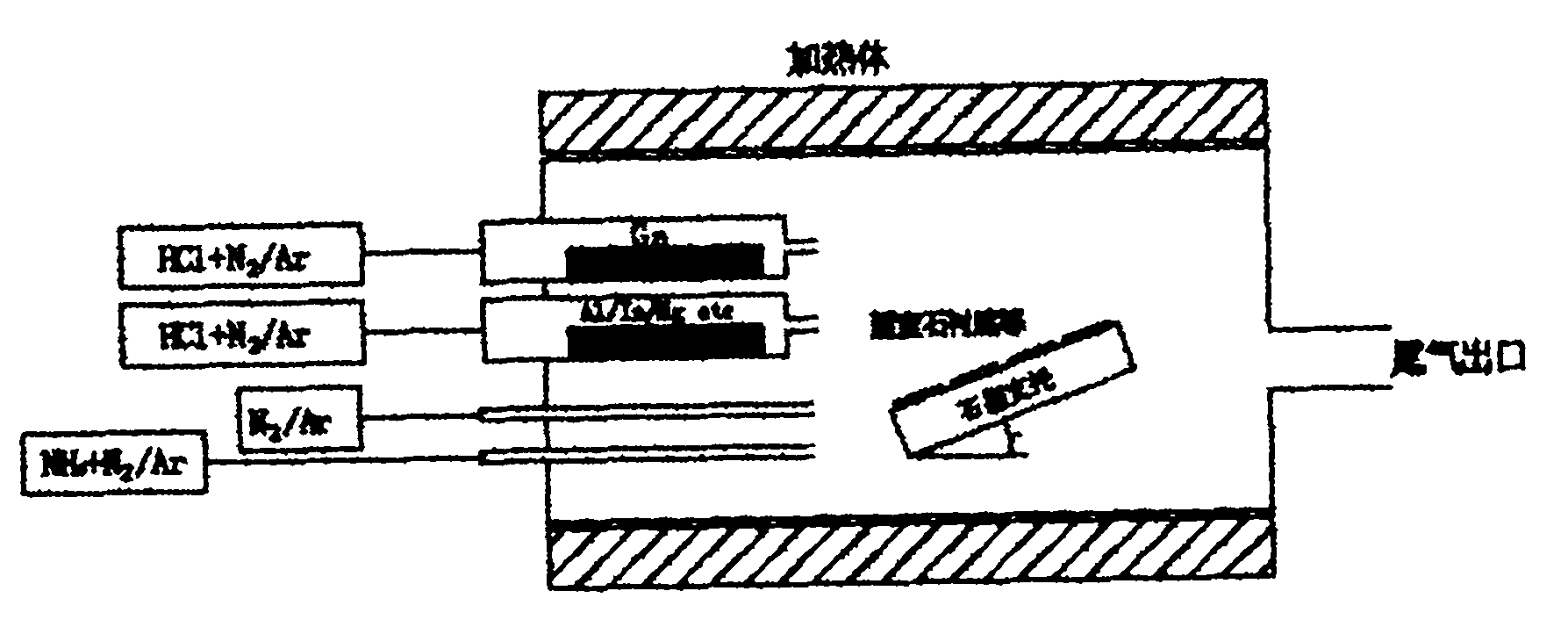
[0014] The HVPE system of the present invention includes several parts: a multi-channel gas transport system to realize the growth or doping of multiple semiconductor alloy materials; a specially designed multi-sheet graphite backing and a corresponding reaction source transport structure. The size of the graphite backing is based on the extension The number of growth substrates ranges from 60X60mm to 350X350mm, independent reaction source delivery pipelines, graphite support tilt / rotation structure, heating system for large-volume growth areas, and quartz shower heads to achieve large-scale growth of semiconductor materials. While increasing the output, it also guarantees the quality of the growth material; the new quartz reaction chamber structure, which is compact in structure, can also achieve HVPE growth of nitride materials when using a single temperature zone, which is energy-saving and efficient. The reaction chamber has a horizontal structure. One end of the reaction ch...


PUM


Abstract

The invention relates to a multi-piece multi-source horizontal hydride vapor phase epitaxy growth system, wherein a reaction chamber is of a horizontal structure, a graphite support is arranged in a growth region, different reaction sources are respectively provided with independent input pipelines, and epitaxy growth substrates are arranged on the graphite support. The multi-piece multi-source horizontal hydride vapor phase epitaxy (HVPE) growth system provided by the invention realizes large-scale application of GaN-based material growth and has the capability of growing multiple pieces of large-area GaN-based materials in one step.

Description

Technical field [0001] The invention relates to a method and device for growing semiconductor materials such as GaN-based materials by multi-sheet hydride vapor phase epitaxy (HVPE), and is a multi-sheet multi-source horizontal hydride vapor phase epitaxy growth system. Background technique [0002] Group III-V nitride materials (also known as GaN-based materials) based on GaN, InGaN, and AlGaN alloy materials are new semiconductor materials that have received much attention internationally in recent years. GaN-based materials are direct bandgap wide bandgap semiconductor materials, with a continuously variable direct band gap between 1.9-6.2eV, excellent physical and chemical stability, high saturation electron drift speed, high breakdown field strength and high thermal conductivity It has important applications in the preparation of short-wavelength semiconductor optoelectronic devices and high-frequency, high-voltage, and high-temperature microelectronic devices. It is used to...

Claims


Application Information

Patent Timeline
Patent Type & Authority Applications(China)
IPC IPC(8): C30B25/14C30B25/20C30B25/10C30B29/40
Inventor 修向前张荣华雪梅谢自力韩平施毅顾书林胡立群郑有炓
Owner NANJING UNIV
Why Eureka
Try Eureka