VDMOS (Vertical Double-diffusion Metal Oxide Semiconductor Structure) device and manufacturing method thereof

A device manufacturing method and device technology, applied in semiconductor/solid-state device manufacturing, semiconductor devices, electrical components, etc., can solve the problem of low theoretical value of electrical properties of VDMOS devices, and achieve improved electrical properties, reduced occupied area, and improved The effect of utilization

Active Publication Date: 2014-01-22
CSMC TECH FAB2 CO LTD
View PDF2 Cites 0 Cited by
  • Summary
  • Abstract
  • Description
  • Claims
  • Application Information

AI Technical Summary

Problems solved by technology

[0009] However, in actual use, the electrical properties of the VDMOS device with the above structure are often lower than the theoretical value

Method used


Image

  • VDMOS (Vertical Double-diffusion Metal Oxide Semiconductor Structure) device and manufacturing method thereof
  • VDMOS (Vertical Double-diffusion Metal Oxide Semiconductor Structure) device and manufacturing method thereof
  • VDMOS (Vertical Double-diffusion Metal Oxide Semiconductor Structure) device and manufacturing method thereof

Examples


Embodiment 1

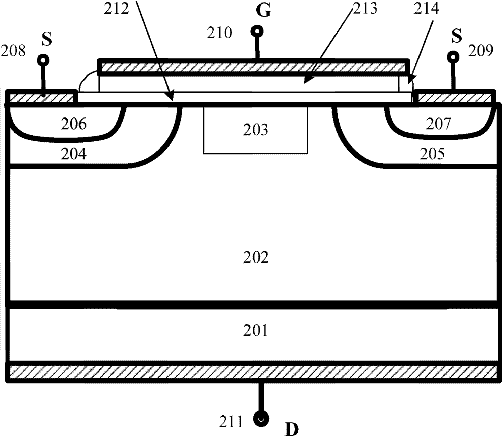
[0046] Based on this, Embodiment 1 of the present invention provides a VDMOS device, the structure of which is as follows figure 2 shown, including:

[0047] a substrate, the substrate includes a body layer 201 and an epitaxial layer 202 located on the body layer, the body layer includes a drain region;

[0048] The isolation region 203 located in the epitaxial layer 202, generally, the isolation region 203 is located in the surface of the epitaxial layer 202, and there is no isolation region material on the surface of the epitaxial layer 202;

[0049] The first body region 204 and the second body region 205 in the epitaxial layer located on both sides of the isolation region 203 have the same doping state as the epitaxial layer. The conductivity type of doping ions is opposite;

[0050] The first source region 206 located in the first body region 204, the second source region 207 located in the second body region 205, the doping states of the first source region 206 and th...

Embodiment 2

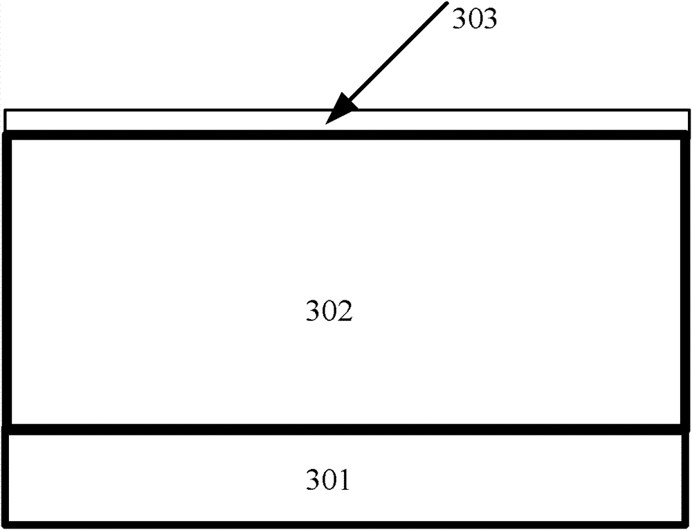
[0064] This embodiment discloses the manufacturing method of the VDMOS device described in the previous embodiment, Figure 3 to Figure 12 It is a sectional view of each step of the method, and the present embodiment only takes an N-type VDMOS device as an example for illustration, and the method includes the following steps:

[0065] Such as image 3 As shown, a substrate is provided, the substrate includes a bulk layer 301 and an epitaxial layer 302 above the bulk layer 301, the bulk layer 301 includes a drain region, and the bulk layer 301 and the epitaxial layer 302 in this embodiment are N-type doped ;

[0066] It should be noted that the substrate in this embodiment may include semiconductor elements, such as silicon or silicon germanium (SiGe) in single crystal, polycrystalline or amorphous structure, and may also include mixed semiconductor structures, such as silicon carbide, indium antimonide , lead telluride, indium arsenide, indium phosphide, gallium arsenide or ...

Embodiment 3

[0092] The VDMOS device manufacturing method disclosed in this embodiment is different from the method for forming an isolation region in the previous embodiment. In this embodiment, the step of forming the isolation region in the surface of the epitaxial layer includes:

[0093] Step 1: forming an opening in the surface of the epitaxial layer;

[0094] In this embodiment, a photolithography process can be used to form an opening pattern on the surface of the epitaxial layer, and then the photoresist layer with the opening is used as a mask to etch away the epitaxial layer material at the opening, so that Form the opening.

[0095] Step 2: covering the surface of the epitaxial layer with an isolation layer to fill the opening with an isolation layer material;

[0096] In this embodiment, chemical vapor deposition or physical vapor deposition can be used to cover the surface of the epitaxial layer with an isolation layer, and HDP (high density plasma chemical vapor deposition)...


PUM

PropertyMeasurementUnit
thicknessaaaaaaaaaa

Abstract

A Vertical Double-diffused Metal-Oxide-Semiconductor (VDMOS) device and a method for fabricating the same are provided. The VDMOS device includes a substrate which includes a body layer (201) and an epitaxial layer (202) formed over the body layer (201). The body layer (201) has a drain region. The VDMOS device further includes an isolating region (203) formed in the epitaxial layer (202), a first body region (204) and a second body region (205) formed in the epitaxial layer (202) and located at two sides of the isolating region (203), a first source region (206) and a second source region (207) formed in the first body region (204) and the second body region (205) respectively, and a gate region formed above the isolating region (203) and located between the first source region (206) and the second source region (207).

Description

technical field [0001] The invention relates to the technical field of semiconductor manufacturing, and more specifically, to a VDMOS device and a manufacturing method thereof. Background technique [0002] With the continuous development of semiconductor technology, VDMOS (Vertical Double-diffuse MOS) devices have low switching loss, high input impedance, low driving power, good frequency characteristics, and highly linear transconductance. And other advantages, are more and more widely used in analog circuits and drive circuits, especially the high-voltage power part. [0003] Existing VDMOS device structures such as figure 1 As shown, taking N-type VDMOS devices as an example, including: [0004] A substrate, the substrate comprising a bulk layer 101 and an epitaxial layer 102 above the bulk layer, the bulk layer 101 comprising a drain region, wherein the bulk layer 101 and the epitaxial layer 102 are N-type doped; [0005] The first body region 103 and the second body...

Claims


Application Information

Patent Timeline
Patent Type & Authority Patents(China)
IPC IPC(8): H01L29/78H01L29/06H01L21/336
CPCH01L29/66719H01L29/7802H01L29/0653H01L21/26533H01L29/0878
Inventor 王乐
Owner CSMC TECH FAB2 CO LTD
Why Eureka
Try Eureka