

Non-scanning type wavelength dispersion X-ray fluorescence spectrometer
A fluorescence spectrometer and wavelength dispersion technology, which is applied in the field of X-ray fluorescence spectrometer, can solve the problems of poor operation stability and adjustment convenience, inability to analyze multiple material components at the same time, low effective utilization of X-rays, etc., and achieve simple structure and volume Small, easy to upgrade and adjust, and improve the effect of effective utilization
- Summary
- Abstract
- Description
- Claims
- Application Information
AI Technical Summary
Problems solved by technology
Method used
Image

Examples
Embodiment 1
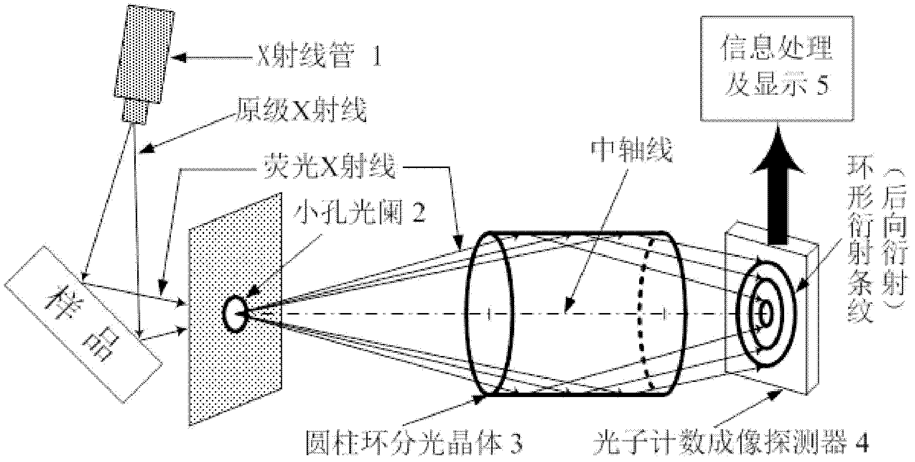
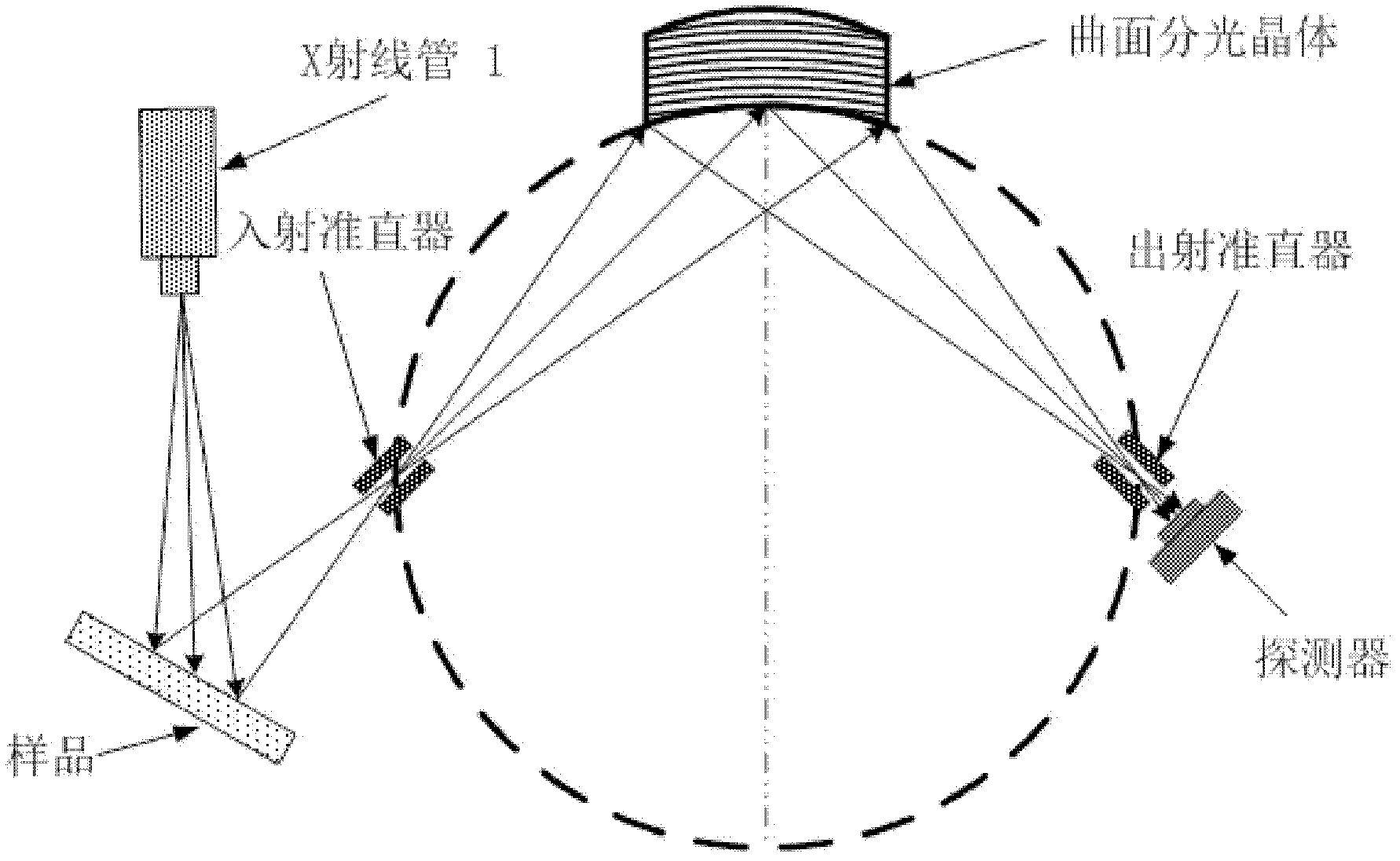
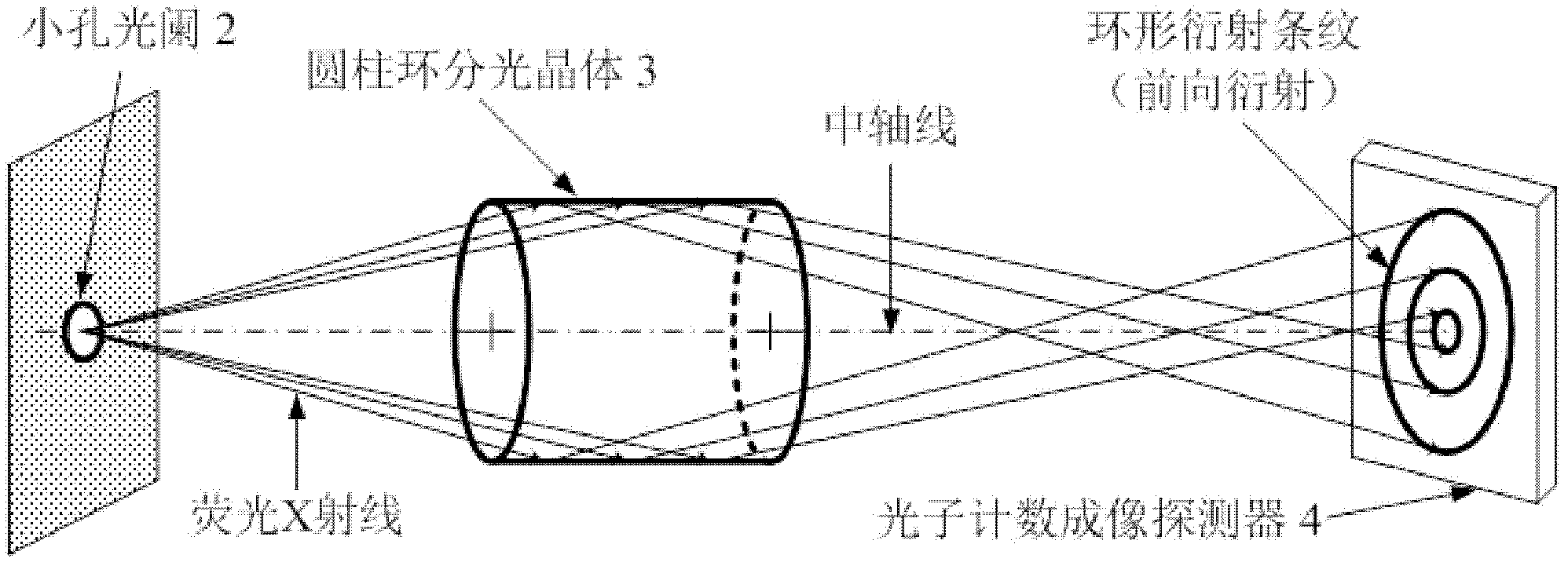
[0044] In this embodiment, a non-scanning wavelength dispersive X-ray fluorescence spectrometer (such as figure 1 shown), is in the traditional scanning wavelength dispersive X-ray fluorescence spectrometer (such as figure 2 (shown) is conceived and designed on the basis of: "small aperture diaphragm 2" is used to replace the traditional "incident collimator + exit collimator" in terms of aperture; in terms of beam splitting system, "cylindrical ring beam splitter crystal 3" is used to replace the traditional "Plane beam-splitting crystal" or "curved beam-splitting crystal"; the detector uses "photon counting imaging detector 4" to replace the traditional "proportional counter" or "scintillation counter" or "semiconductor detector"; Angle measuring device and displacement mechanism (or rotation mechanism).
[0045] like figure 1 As shown, the X-ray fluorescence spectrometer is mainly composed of an X-ray tube 1, an aperture diaphragm 2, a cylindrical ring spectroscopic crys...
Embodiment 2
[0065] This embodiment is basically the same as Embodiment 1, the difference is that on the basis of the photon counting imaging detector 4 described in Embodiment 1, a semiconductor layer can be added between the output end of the MCP and the position-sensitive anode, and the MCP There is a gap between the output terminal and the semiconductor layer, the semiconductor layer is plated on the insulating substrate, and the DC high-voltage power supply is electrically connected to the semiconductor layer through high-voltage leads or conductive electrodes (such as Figure 5 shown). At this time, the above step S540, that is, the physical process of collecting the electron cloud by the position-sensitive anode, evolves into: the electron cloud first crosses to the semiconductor layer under the action of the accelerating bias electric field, and then is induced to the position-sensitive anode through charge induction.
Embodiment 3
[0067] This embodiment is basically the same as Embodiment 1, the difference is: on the basis of the X-ray fluorescence spectrometer described in Embodiment 1, according to the power consumption of X-ray tube 1, it can be equipped with a corresponding high-voltage generator and voltage regulator Steady flow device and cooling system to meet the actual application needs.
PUM
 Abstract
Description
Claims
Application Information