Method for preparing low-stress micro-tensile test sample with mesh support frame

A supporting frame and micro-stretching technology, which is applied in the field of preparation of low-stress micro-tensile specimens, can solve the problems of incompatibility with the preparation process of Cu-TSV micro-tensile specimens, cumbersome data processing, etc., and achieve the dispersion of shear stress , reduce the shear area, reduce the effect of stress deformation

Inactive Publication Date: 2012-06-27
SHANGHAI JIAO TONG UNIV
View PDF2 Cites 13 Cited by
  • Summary
  • Abstract
  • Description
  • Claims
  • Application Information

AI Technical Summary

Problems solved by technology

The disadvantage of this method is that it needs to be stretched twice to subtract the force generated by stretching the microspring, resulting in cumbersome data processing
Moreover, the Cu sputtering layer is used as the seed layer in the preparation method, which is not compatible with the preparation process of Cu-TSV micro-tensile specimens.

Method used


Image

  • Method for preparing low-stress micro-tensile test sample with mesh support frame
  • Method for preparing low-stress micro-tensile test sample with mesh support frame
  • Method for preparing low-stress micro-tensile test sample with mesh support frame

Examples


Embodiment 1

[0031] (1) After cleaning the 3-inch glass substrate, spin-coat AZ4630 photoresist at a speed of 1200 rpm for 30 seconds as a sacrificial layer, with a thickness of about 10 μm, and then pre-bake it at 110°C 1h to improve the bonding force between photoresist sacrificial layer and glass substrate and subsequent metal layer;

[0032] (2) 0.8 μm metal Ti is sputtered on the photoresist sacrificial layer, and the glass substrate is placed in 5Vol.% glacial acetic acid, 1Vol.% hydrofluoric acid, 1Vol.% hydrogen peroxide and 0.05wt% dodecylsulfonic acid Perform Ti surface activation treatment in a mixed solution of sodium for 50s, and then bake at 60°C for 30min;

[0033] (3) Throw AZ4630 photoresist at a speed of 1200 rpm on the surface activation treatment Ti layer for 30 seconds, then sequentially perform exposure and development for 150s, and realize micro-stretching according to the shape of the micro-stretching sample designed by the mask plate Patterning of the photoresist ...

Embodiment 2

[0039] (1) After cleaning the 4-inch glass substrate, repeat the spin-coating photoresist treatment and drying treatment as in step (1) in Example 1;

[0040] (2) sputtering on photoresist sacrificial layer Metal Ti, repeat the Ti surface activation treatment and oven dry treatment as step (2) among the embodiment 1;

[0041] (3) According to the method of step (3) in embodiment 1, obtain the patterning of microtensile sample layer photoresist structure;

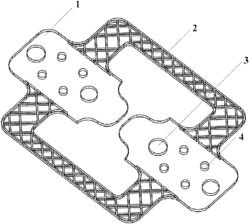
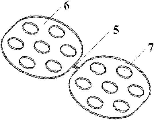
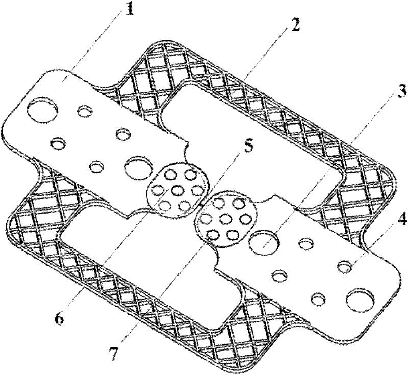
[0042] (4) Utilize the electrochemical deposition technology, on the titanium hydride film layer that has been processed, at the electroplating temperature of 20 ℃, the plating solution stirring speed of 350 rpm, 5mA / cm 2 Under the condition of the current density, using methanesulfonate copper plating solution to electroplate out Figure 4 The Cu-TSV micro-tensile sample layer in the medium includes a micro-tensile sample 5 and a rectangular support platform 8, and its thickness is 6 μm;

[0043] (5) According to the meth...

Embodiment 3

[0046] (1) After the 6-inch glass substrate is cleaned, repeat the spin-coating photoresist treatment and drying treatment of step (1) in Example 1;

[0047] (2) Sputtering on photoresist sacrificial layer Metal Ti, repeat the Ti surface activation treatment and oven dry treatment as step (2) among the embodiment 1;

[0048] (3) According to the method of step (3) in Example 1, the patterning of the photoresist structure of the micro-tensile sample layer is obtained, the shape of the micro-tensile sample layer array is basically consistent with the shape of the support frame layer, only Reserve a processing gap of 100 μm at both ends of the film sample;

[0049] (4) Utilize the electrochemical deposition technology, on the titanium hydride film layer that has been processed, at the electroplating temperature of 20 ℃, the plating solution stirring speed of 350 rpm, 15mA / cm 2 Under the condition of the current density, using methanesulfonate copper plating solution to electro...


PUM

PropertyMeasurementUnit
thicknessaaaaaaaaaa
thicknessaaaaaaaaaa
thicknessaaaaaaaaaa

Abstract

The invention discloses a method for preparing a low-stress micro-tensile test sample with a mesh support frame, relating to the technical field of testing of films. The method comprises the following steps of: spinning photoresist on a glass substrate used as a sacrificial layer to be pre-baked, sputtering a metal Ti layer on the sacrificial layer, carrying out surface activation treatment of the sacrificial layer used as a seeding layer, and spinning, exposing and developing on the seeding layer; realizing imaging of a photoresist structure according to the shape of a micro-tensile test sample layer designed by a mask template; electroplating a Cu-TSV (Through Silicon Via) test sample layer on the Ti layer with the activated surface; carrying out electrochemical deposition of a support frame layer on the Cu-TSV plated layer; and finally, removing a photoresist graphical layer, a Ti sputtered layer and the sacrificial layer to obtain an independent suspension Cu-TSV micro-tensile test sample with the mesh support frame. The micro-tensile test sample prepared by using the method disclosed by the invention is capable of effectively reducing the film stress and has the advantages of being simple in structure, easy for preparation and low in cost; therefore, the in-situ independent tension of the Cu-TSV film is realized, and the micro-tensile test sample is beneficial to a micro-tensile precise test.

Description

technical field [0001] The invention relates to a method for preparing a micro-tensile sample in the technical field of testing, in particular to a low-pressure test sample with a mesh support frame for testing the mechanical properties of through-silicon via copper (Cu-TSV) films. Method for preparing stress microtensile specimens. Background technique [0002] With the miniaturization trend of electronic products in the microelectronics industry, the concept of three-dimensional integration of chips has emerged as the times require, and is realized through silicon via (TSV-through silicon via) technology. Copper was chosen as the interconnect material in TSVs due to its high electrical conductivity, relatively mature electrodeposition process, and its high resistance to electron migration. However, the mechanical properties of materials at the microscale are not only affected by size effects, but also vary depending on the fabrication process, i.e., the mechanical propert...

Claims


Application Information

Patent Timeline
Patent Type & Authority Applications(China)
IPC IPC(8): G01N1/28
Inventor 汪红李君翊王慧颖王艳丁桂甫
Owner SHANGHAI JIAO TONG UNIV
Why Eureka
Try Eureka