Digital holographic detection device for subsurface defect of optical element

A subsurface defect, digital holographic technology, applied in optical testing flaws/defects, phase influence characteristic measurement, etc., can solve problems such as low detection efficiency, limited practicability, and inability to achieve quantitative analysis

Inactive Publication Date: 2012-06-27
SHANGHAI UNIV
View PDF4 Cites 26 Cited by
  • Summary
  • Abstract
  • Description
  • Claims
  • Application Information

AI Technical Summary

Problems solved by technology

The current detection methods include: (1) The detection method based on the combination of acid etching and confocal microscopy technology, although it is easy to observe the existence of defects, but due to the inhomogeneity of acid etching rate and surface roughness, it can only be used for isotropic Homogeneous materials have poor applicability, and the acid etching process will bring unpredictable damage to the components; (2) The method based on the combination of quantum fluorescence and confocal microscopy detection technology has high precision, but it needs to be

Method used


Image

  • Digital holographic detection device for subsurface defect of optical element
  • Digital holographic detection device for subsurface defect of optical element
  • Digital holographic detection device for subsurface defect of optical element

Examples


Embodiment 1

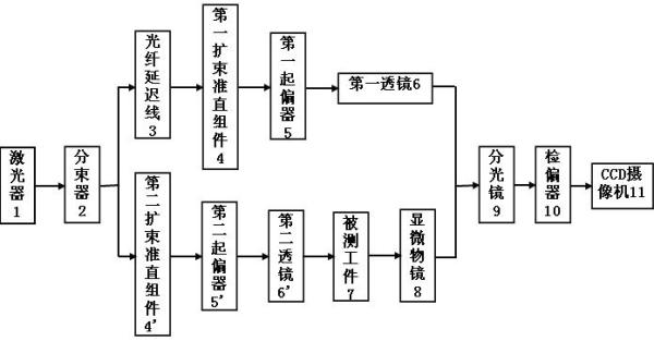
[0024] Embodiment one: figure 1 The optical element subsurface defect detection device shown is a structural block diagram of this implementation, consisting of figure 1 It can be seen that the device consists of a laser 1, a beam splitter 2, a fiber delay line 3, the first and second two beam expander collimation components 4, 4', the first and second two polarizers 5, 5 ', the first and second lenses 6, 6', a microscope objective lens 8, a beam splitter 9, an analyzer 10 and a CCD camera 11.

[0025] For implementation steps see image 3 , the beam emitted by the laser 1 is divided into two beams by the beam splitter 2, one beam is the measurement beam and the other is the reference beam, the reference beam passes through the fiber delay line 3, and then the two beams are collimated through the first and second beam expanders of their respective optical paths Components 4, 4', first and second polarizers 5, 5' and first and second lenses 6, 6', and then the measuring beam...

Embodiment 2

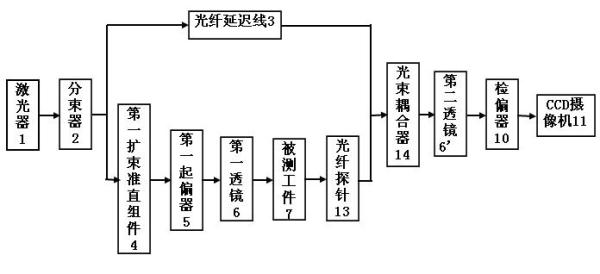
[0026] Embodiment two: figure 2 The optical element subsurface defect detection device shown is a structural block diagram of this implementation, consisting of figure 2 It can be seen that this set consists of a laser 1, a beam splitter 2, a fiber delay line 3, a first beam expander collimator assembly 4, a first polarizer 5, a first and a second lens 6, 6', a A fiber probe 13, a beam coupler 14, a polarizer 10 and a CCD camera 11 are composed.

[0027] For implementation steps see Figure 4 : The beam emitted by the laser 1 is divided into two beams by the beam splitter 2, one beam is used as the measurement beam and the other is used as the reference beam, the reference beam passes through the fiber delay line 3, the measurement beam passes through the first beam expander and collimator assembly 4, and the first polarizer 5 and the first lens 6 are then irradiated on the workpiece 7 to be measured, reflected by the workpiece 7, and the reflected light is detected by the...


PUM


Abstract

The invention relates to a digital holographic detection device for a subsurface defect of an optical element. A light beam in the device is divided into a measuring light beam and a reference light beam, so that a measuring light path is obliquely incident to an object to be measured and symmetrically receives reflected light, the reflected light interferes with reference light, scattered light information of the subsurface defect is acquired from an interference pattern, the direct reflected light on the surface and stray light in a system are inhibited, and the scattered light information of the subsurface defect of the optical element is acquired. The detection device has the characteristics that: (1) a light source is a short coherent light source, so that the stray light in the system can be inhibited; (2) the measuring light path in the device is obliquely incident and symmetrically receives the reflected light, so that the direct reflected light on the surface of the optical element can be inhibited, only scattered light from the subsurface defect is received, and the signal-to-noise ratio of a signal is improved; (3) an optical fiber probe in the device is used for receiving the scattered light information, so that the limitation that a high-rate microscope objective is used for receiving the subsurface defect is overcome; and (4) the acquired image is analyzed and processed according to a digital holographic calculation principle, so that the quantitative depth information of the subsurface defect is acquired.

Description

technical field [0001] The invention relates to a digital holographic detection device for optical element subsurface defects. The invention uses a short coherent light source to obtain the scattered light information of the subsurface defect of the optical element through oblique incidence and symmetrical reception, and interferes with the reference beam; then uses the principle of digital holography to calculate and analyze the morphology and depth distribution of the subsurface defect quantitative information. The device of the invention is mainly used to realize the detection of subsurface defects of smooth optical elements. Background technique [0002] Subsurface defects of optical components are tree-like complex structures located in submicron to micron depths below the surface of the component. They are mainly divided into scratches, cracks and impurities, etc., and the extension depth can reach tens of microns to hundreds of microns. High-precision and efficient ...

Claims


Application Information

Patent Timeline
IPC IPC(8): G01N21/88G01N21/45
Inventor 于瀛洁伍小燕涂桥王驰
Owner SHANGHAI UNIV
Why Eureka
Try Eureka