Planar spiral inductor with wide-narrow-alternatingly line width and space

A planar spiral and spiral inductance technology, applied in the field of electronics, can solve the problems of a single change in the metal wire spacing and line width of the spiral inductance, reduce the mutual inductance of the spiral inductance coil, and the inductance value is not significantly improved, etc. Improve the inductance Q value and overcome the effect of the inductance Q value being too low

Inactive Publication Date: 2012-06-27
XIDIAN UNIV
View PDF4 Cites 25 Cited by
  • Summary
  • Abstract
  • Description
  • Claims
  • Application Information

AI Technical Summary

Problems solved by technology

However, the shortcomings of this patent application are: the mutual inductance between the metal coils is reduced, resulting in a low inductance value, and the processing technology is more difficult
However, the shortcomings of this patent application are: the size of the spiral inductor is too large, which does not meet the small size and high integration design requirements of today's radio frequency integrated circuits, the metal line spacing and line width of the spiral inductor have a s

Method used


Image

  • Planar spiral inductor with wide-narrow-alternatingly line width and space
  • Planar spiral inductor with wide-narrow-alternatingly line width and space
  • Planar spiral inductor with wide-narrow-alternatingly line width and space

Examples


Embodiment Construction

[0021] The present invention will be described in further detail below in conjunction with the accompanying drawings.

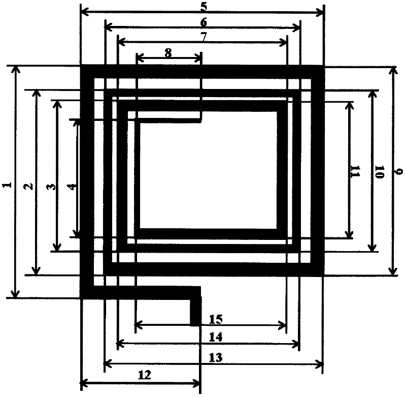
[0022] figure 1 The shown planar spiral inductor with alternating line width and spacing structure includes a silicon substrate, an insulating layer, a bottom metal layer of the planar spiral inductor, through holes, and a metal layer of the planar spiral inductor. A layer of 1 μm thick oxide is grown on a 450 μm thick silicon base to form an insulating layer, a layer of 10 nm thick titanium gold film is sputtered on the insulating layer, and a 500 nm thick metal film is plated on the surface of the titanium gold film, etched Metal film, forming the bottom metal layer of the spiral inductor, depositing a 900nm thick oxide on the bottom metal layer of the spiral inductor to form an insulating layer, etching the insulating layer to form a through hole, and plating a 2μm thick metal film on the insulating layer, selectively Etching forms the spiral inductor met...


PUM

PropertyMeasurementUnit
Line widthaaaaaaaaaa
Outer diameteraaaaaaaaaa

Abstract

The invention discloses a planar spiral inductor with wide-narrow-alternatingly line width and space, which can be used for an RF integrated circuit. The planar spiral inductor adopts the structure that a spiral inductive insulation layer is arranged on a silicon substrate; the metal thin film is coated on the insulation layer to etch an inductive bottom layer metal layer, so the insulation layeris deposited on the bottom layer metal layer; through holes are formed on the insulation layer so as to connect the bottom layer metal layer and the spiral inductor layer; and the metal thin film is coated on the insulation layer to etch a spiral inductive metal layer with a multi-turn coil; and the pattern of the coil is formed through conductive metal. According to the invention, the metal coilis alternately changed in width form the outer ring to the inner ring, whereas the space is alternately changed in width form the inner ring to the outer ring, thereby reducing the Ohm wastage causedby equivalent resistors connected in series, lowering the proximity effect of the metal wires, improving the quality factor Q value of the spiral inductor, increasing the mutual induction of the wirecoils, and also improving the inductance value of the spiral inductor.

Description

technical field [0001] The invention belongs to the field of electronic technology, and further relates to a planar spiral inductor with alternating line width and spacing structure in the field of microelectronic technology. The metal line width and spacing of the invention adopts a width-narrow alternating structure, which can be used in the fields of microwave integrated circuits, filter nets, radio frequency transceiver circuits, LC oscillators, radio frequency ICs and the like. Background technique [0002] With the development of the field of radio frequency integrated circuits, the demand for high-performance planar spiral inductors is increasingly urgent. Whether spiral inductors can obtain high quality factor Q value and high inductance value has become a research hotspot in the field of microelectronics technology. [0003] At present, there are two main methods to improve the performance of planar spiral inductors: one is to optimize the structural parameters. By...

Claims


Application Information

Patent Timeline
IPC IPC(8): H01F17/02
Inventor 田文超孙昊杨银堂
Owner XIDIAN UNIV
Why Eureka
Try Eureka