A New Manufacturing Method of Planar Spiral Inductor

A flat spiral and production method technology, applied in the new production field of flat spiral inductors, can solve problems such as inductances that are difficult to achieve high Q value and S21 parameters, the thickness of the inductor coil metal layer is limited, and the loss of the substrate increases, and the device can be achieved. Ease of control of performance consistency, avoidance of conduction currents and eddy current effects, reduced substrate losses

Active Publication Date: 2018-11-06
BEIJING MXTRONICS CORP +1
View PDF4 Cites 0 Cited by
  • Summary
  • Abstract
  • Description
  • Claims
  • Application Information

AI Technical Summary

Problems solved by technology

At present, planar spiral inductors are fabricated on a silicon substrate using a CMOS process, but the planar spiral inductors produced by this method have inherent defects, such as limited by the integrated circuit deposition process, the metal layer of the inductor coil The thickness is limited, so that the loss of the coil is large, and due to the semiconductor characteristics of silicon, the strong coupling and skin effect between the coil and the silicon substrate at high frequencies further increase the substrate loss
Therefore, it is difficult to realize an inductor with a high Q value and S21 parameter on a silicon substrate using a CMOS process. The Q value is generally below 3, and the S21 parameter is below 0.5.

Method used


Image

  • A New Manufacturing Method of Planar Spiral Inductor
  • A New Manufacturing Method of Planar Spiral Inductor
  • A New Manufacturing Method of Planar Spiral Inductor

Examples


Embodiment Construction
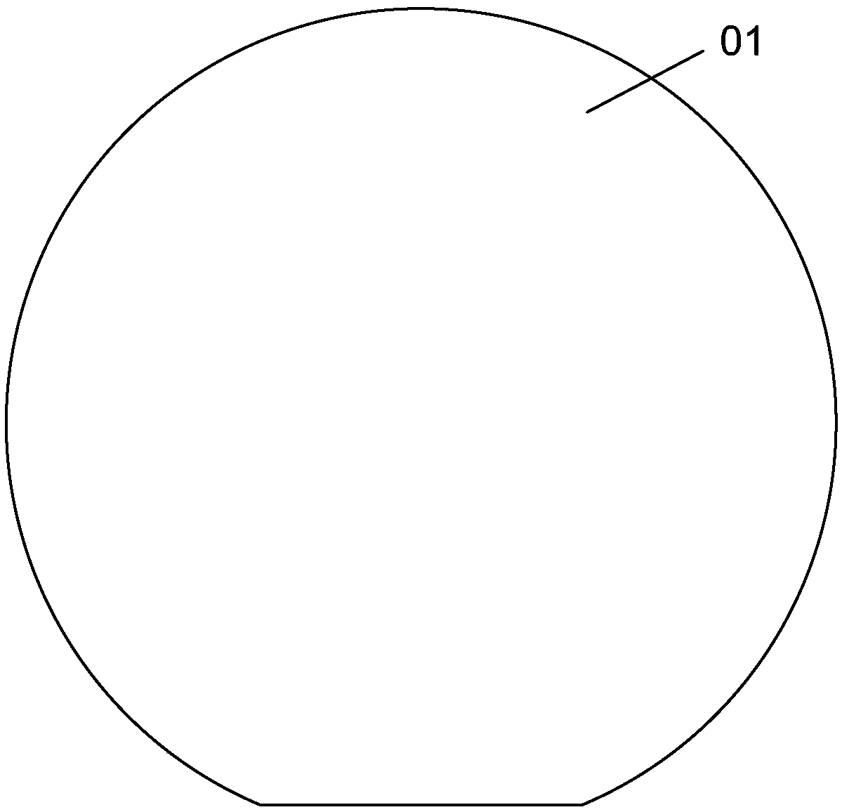
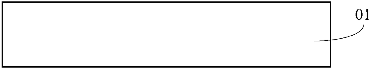
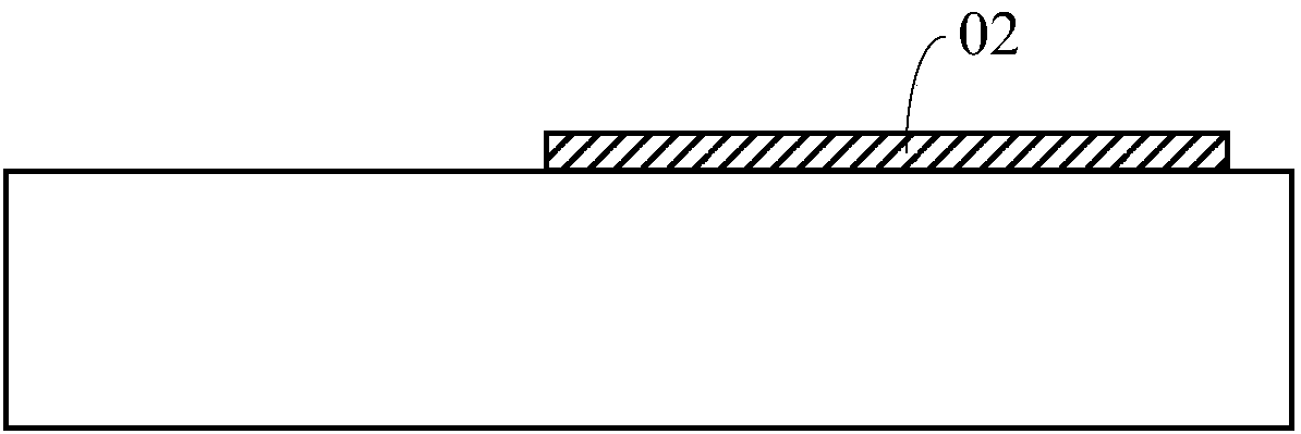
[0035] The basic idea of ​​the invention is: the invention relates to a novel manufacturing method of a planar spiral inductor. The manufacturing method, the steps are as follows: ① use glass or quartz substrate to carry out the manufacture of planar spiral inductors; ② use MEMS technology, including metal film deposition process, dielectric layer film deposition process, thick metal layer electroplating process, thick glue light Engraving process, etching process, etc. to realize the production of planar spiral inductors; ③ There is no need for a thick insulating layer to isolate the planar spiral inductor from the substrate; ④ The planar shape and coil thickness of the planar spiral inductor are not limited. The present invention uses MEMS technology to realize the fabrication of planar spiral inductors on glass or quartz substrates, avoids the coupling and skin effect between the coil and the substrate at high frequencies, and can realize high-Q inductance, while the inducta...


PUM

PropertyMeasurementUnit
thicknessaaaaaaaaaa
thicknessaaaaaaaaaa

Abstract

The invention relates to a novel manufacturing method of a planar spiral inductor. Manufacturing of the planar spiral inductor is carried out through a glass or quartz substrate; manufacturing of the planar spiral inductor is achieved by an MEMS technology which comprises a metal thin film deposition process, a dielectric layer thin film deposition technology, a thick metal layer plating process, a thick resist lithography process, an etching process and the like; the planar spiral inductor and the substrate do not need to be isolated by a thick insulating layer; and the plane shape of the planar spiral inductor and the thickness of a coil are not limited. Manufacturing of the planar spiral inductor is achieved by the MEMS technology on the glass or quartz substrate; the coupling effect and the skin effect between the coil and the substrate at a high frequency are avoided; a high Q-value inductor can be achieved; meanwhile, the thickness of a metal layer of an inductance coil is not limited; and the loss of the coil is low. The technology is simple; the requirements of multiple fields of a signal isolator, a planar antenna, a microwave baseband line, a planar spiral inductor resonator and the like can be met; and the process difficulty is reduced.

Description

technical field [0001] The invention relates to a manufacturing method of a planar spiral inductor, in particular to a novel manufacturing method of a planar spiral inductor. Background technique [0002] Radio frequency integrated circuits require high-quality passive components, such as inductors, capacitors, etc., in which inductors are generally replaced by equivalent inductors formed by operational amplifiers, but due to their large power consumption, large area, large noise, and poor high-frequency performance It cannot meet the needs of growing development, which makes the urgency of researching high-quality inductors increase, and thus the spiral inductors with planar structure were born. The quality factor (Q) essentially characterizes the energy loss of the reactance element, and it is an important indicator to measure the performance of the inductor. At present, planar spiral inductors are fabricated on a silicon substrate using a CMOS process, but the planar spi...

Claims


Application Information

Patent Timeline
Patent Type & Authority Patents(China)
IPC IPC(8): H01L23/64B81C1/00
Inventor 杨静张富强孟美玉李光北王碧
Owner BEIJING MXTRONICS CORP
Why Eureka
Try Eureka