

Method for preparing nano texture through local anodic oxidation
A local anodizing and nanotexturing technology, applied in the manufacture of microstructure devices, microstructure technology, gaseous chemical plating, etc., can solve the problems of micro-friction, adhesion, affecting operation and service life, etc., to reduce surface adhesion strength, good anti-adhesion performance
- Summary
- Abstract
- Description
- Claims
- Application Information
AI Technical Summary
Problems solved by technology
Method used
Image

Examples
Embodiment 1
[0015] Preparation of Hydroxylated Single Crystal Silicon Surface First soak the single crystal silicon surface of the single crystal silicon wafer in 1% HF aqueous solution for hydrogen passivation for 4 minutes; take out the hydrogen passivated single crystal silicon wafer , ultrasonically cleaned in deionized water, and then blown dry with nitrogen;
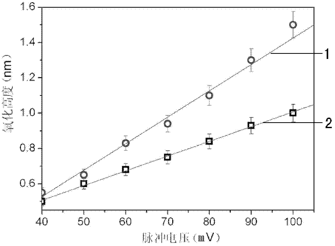
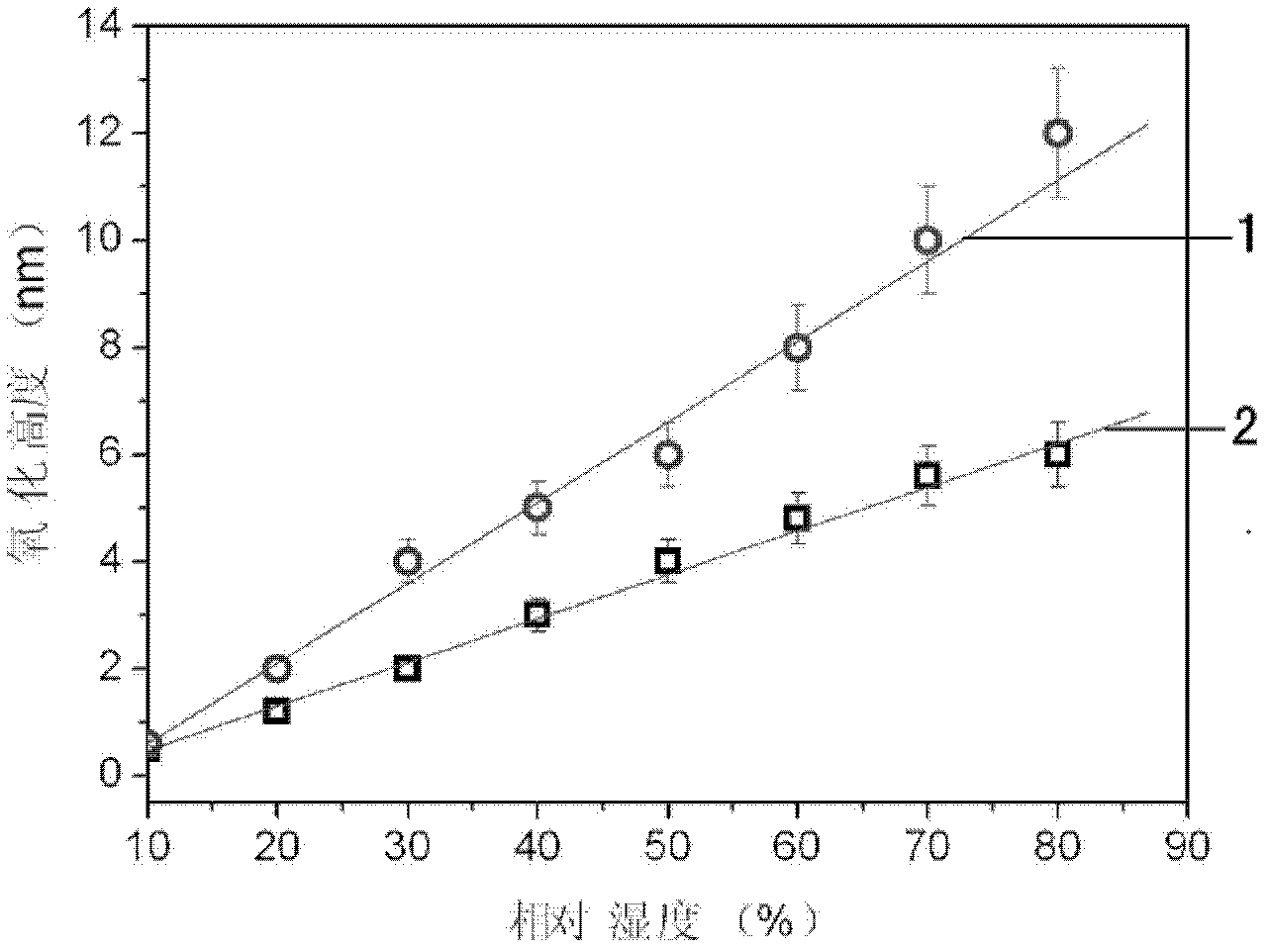
[0016] The preparation of surface nano-texture edited the computer script according to the preset pattern, and imported the computer script into the online control software (SPM console, the same for the following examples) of the conductive atomic force microscope (model CSPM 4000, the same for the following examples), Draw a circular pattern with a preset surface coverage of 15%; operate a conductive atomic force microscope, and perform oxidation processing under the conditions of a controlled pulse voltage of 40mV, a pulse width of 50ms and a relative humidity of 15%, and the processed single crystal silicon wafer The sur...
Embodiment 2
[0018] Preparation of Hydroxylated Single Crystal Silicon Surface First soak the single crystal silicon surface of the single crystal silicon wafer in 2% HF aqueous solution for hydrogen passivation for 2 minutes; take out the hydrogen passivated single crystal silicon wafer , ultrasonically cleaned in deionized water, and then blown dry with nitrogen;
[0019] Preparation of surface nano-texture Edit the computer script according to the preset pattern, import the computer script into the online control software of the conductive atomic force microscope, and draw a triangle figure with a preset surface coverage rate of 18%; operate the conductive atomic force microscope , under the conditions of controlling the pulse voltage of 70mV, the pulse width of 80ms and the relative humidity of 65%, the oxidation process was carried out, and the nano-texture on the surface of the processed single crystal silicon wafer was confirmed by scanning with a conductive atomic force microscope...
Embodiment 3
[0021] Preparation of Hydroxylated Single Crystal Silicon Surface First soak the single crystal silicon surface of the single crystal silicon wafer in 2% HF aqueous solution for hydrogen passivation for 2 minutes; take out the hydrogen passivated single crystal silicon wafer , ultrasonically cleaned in deionized water, and then blown dry with nitrogen;
[0022] Preparation of surface nano-texture Edit the computer script according to the preset pattern, import the computer script into the online control software of the conductive atomic force microscope, draw a preset rectangular figure with a surface coverage of 20%; operate the conductive atomic force microscope , under the conditions of controlling the pulse voltage of 80mV, the pulse width of 90ms and the relative humidity of 85%, the oxidation process was carried out, and the nano-texture on the surface of the processed single crystal silicon wafer was confirmed by scanning with a conductive atomic force microscope, and ...
PUM
 Abstract
Description
Claims
Application Information